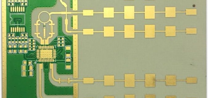
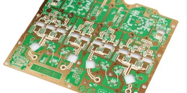
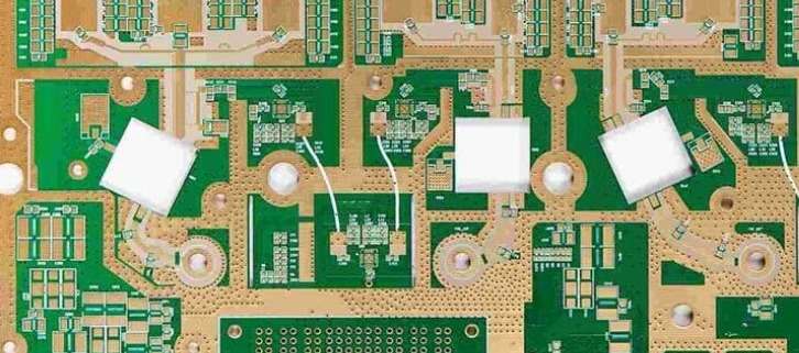
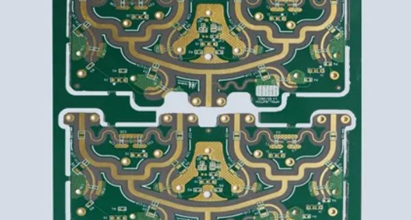
Printed Circuit Boards (PCBs) are essential in modern electronics, providing the physical structure to connect electronic components and ensuring reliable electrical signals in devices like smartphones, computers, and medical equipment. Among the various types, Rogers PCBs are renowned for their superior performance in high-frequency applications, offering low signal loss, excellent thermal stability, and high electrical reliability. These attributes make them ideal for demanding fields like RF communication, radar systems, and satellite technology. An advanced variation, the Integrated Press Hole Rogers PCB, combines traditional drilling with an integrated press hole process, enhancing both manufacturing efficiency and electrical performance. This technology is particularly valuable in specialized applications, such as 5G networks, high-speed communications, and automotive radar systems, where high-frequency signal integrity and thermal management are crucial.
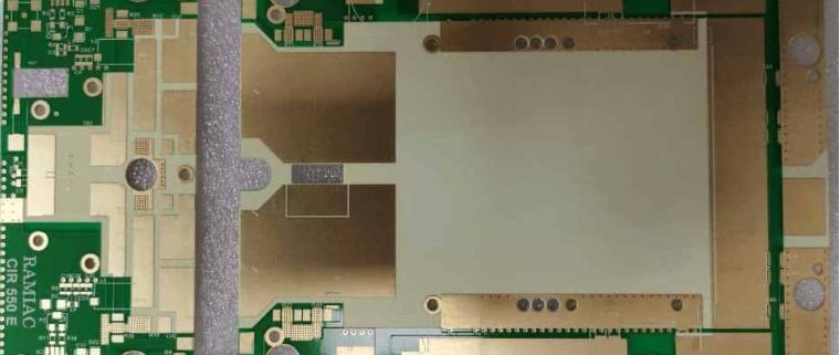
High-speed press hole Rogers PCB refers to a specialized printed circuit board that utilizes Rogers Corporation’s high-frequency laminate materials combined with advanced press hole technology to maintain signal integrity in high-speed applications. Rogers PCB materials, such as RO4003C, RO5880 LZ, and RO3003, are known for their low dielectric loss, high thermal stability, and superior frequency performance, making them ideal for RF and microwave applications. Press hole technology involves precisely drilled holes that facilitate electrical and mechanical connections while minimizing parasitic effects. In high-speed circuits, press holes play a critical role in reducing signal reflections, maintaining impedance control, and ensuring reliable performance. The importance of high-speed press hole technology lies in its ability to enhance signal accuracy, reduce crosstalk, and minimize electromagnetic interference (EMI), making it indispensable for applications such as 5G communication systems, high-frequency radar, and aerospace electronics.
High-speed PCBs are specialized circuit boards designed to handle signals with frequencies exceeding 1 GHz, where signal integrity and impedance control are critical for optimal performance. As modern electronics continue to advance in complexity, the demand for reliable high-speed PCB material Rogers has grown significantly. The choice of material plays a pivotal role in minimizing signal loss, ensuring low dielectric constant (Dk) variability, and maintaining stable impedance, which directly impacts system efficiency. Rogers Corporation, a global leader in high-frequency and high-speed PCB materials, offers innovative laminates that excel in signal integrity and thermal management. Popular Rogers materials used in high-speed PCB design include RO4003C, RO4350B, RT/duroid 5880 LZ, and RO3003, each tailored for applications requiring superior electrical performance and durability. Rogers’ continued innovation makes it the preferred choice for designers developing high-frequency and high-speed PCB solutions.
High-frequency PCBs play a crucial role in RF (Radio Frequency) and microwave applications, where maintaining signal integrity and minimizing signal loss are paramount. These PCBs are essential for industries such as aerospace, telecommunications, and automotive radar systems, where high-frequency signal transmission requires precision and stability. Among the available materials, high frequency Rogers ceramic PCB stands out as a top choice due to its superior dielectric properties, low loss tangent, and excellent thermal performance. Rogers Ceramic PCB materials, such as RO3003G2 and RO5880, provide consistent performance across a wide frequency range, making them ideal for demanding RF environments. Rogers Corporation, a global leader in high-performance laminates, has built a solid reputation by offering innovative PCB solutions that meet the stringent requirements of high-frequency applications. As technology continues to advance, high frequency Rogers ceramic PCB solutions remain the preferred choice for ensuring reliable and efficient signal transmission.
High-frequency Rogers 4003C PCB is a specialized laminate material widely used in RF and microwave applications where signal integrity is critical. Unlike standard FR-4 PCBs, which suffer from higher signal loss and inconsistent dielectric properties at high frequencies, high-frequency Rogers 4003C PCB offers a low dielectric constant (Dk) of 3.38 ± 0.05 and a minimal dissipation factor (Df) of 0.0027 at 10 GHz. This ensures consistent performance across a wide frequency range.
In modern electronics, high-frequency PCBs are crucial for applications like wireless communication, radar systems, and IoT devices, where preserving signal quality and minimizing loss are essential. Rogers 4003C material offers high thermal stability, low moisture absorption, and excellent dimensional stability, making it a top choice for demanding high-frequency applications. As industries advance towards faster data transmission and higher frequency operations, this material continues to be a leading solution for ensuring reliable and efficient performance.
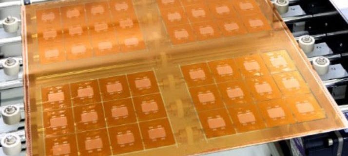
A Custom Glass Class Package Substrate is a type of advanced packaging substrate that utilizes glass as the primary material instead of traditional organic substrates or copper-clad laminates. Glass package substrates offer superior dimensional stability, excellent electrical performance, and high precision, making them ideal for applications that require ultra-fine line/space features.
In comparison to organic substrates, glass substrates provide lower dielectric loss, enabling better signal integrity at higher frequencies. Unlike copper-clad laminates, glass substrates exhibit a coefficient of thermal expansion (CTE) that closely matches silicon chips, reducing the risk of thermal stress and warping.
As semiconductor devices evolve with higher integration and smaller geometries, glass substrate solutions are gaining traction due to their ability to meet the increasing demands of 5G, high-performance computing (HPC), and AI/ML applications. Their unique advantages position them as a promising alternative in the future of advanced semiconductor packaging.
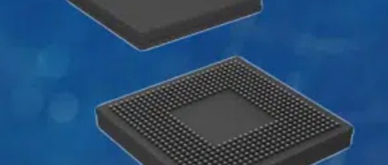
In semiconductor packaging, IC substrates play a crucial role as the interface between the silicon die and the printed circuit board (PCB), ensuring efficient electrical connections, heat dissipation, and mechanical support. As electronic devices become smaller and more complex, the need for high-performance packaging solutions has grown significantly. Among these, Ball Grid Array (BGA) technology has become a dominant choice due to its ability to offer higher pin counts, improved thermal performance, and superior electrical characteristics compared to traditional leaded packages. BGA is widely used in applications ranging from consumer electronics to high-performance computing, where reliability and performance are paramount. To meet the evolving demands of advanced electronics, Custom BGA/IC substrates have emerged as a vital solution. Customization enables manufacturers to optimize substrate designs for specific performance needs, miniaturization challenges, and reliability requirements, ensuring that devices meet the high standards of next-generation applications in AI, IoT, and high-speed computing. 阅读更多
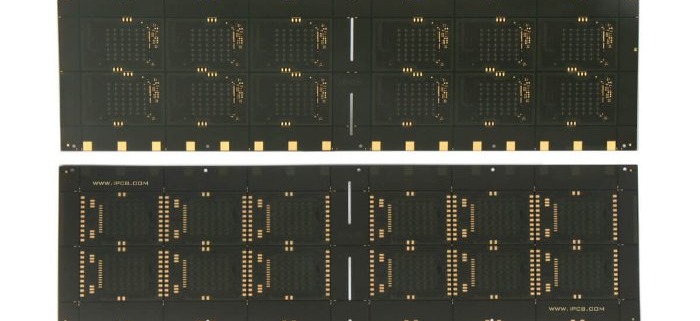
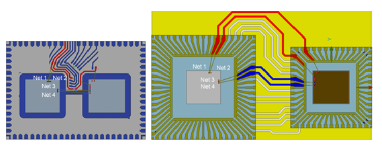
Lead frames are essential components in semiconductor packaging, providing both mechanical support and electrical connections between the silicon chip and the external circuit board. As electronics evolve towards smaller, more powerful devices, the need for advanced lead frame solutions has grown. Custom QFN/QFP Lead Frame designs play a crucial role in this, offering optimized thermal performance, electrical conductivity, and design flexibility. QFN (Quad Flat No-Lead) lead frames are ideal for applications requiring enhanced heat dissipation and reduced signal interference, while QFP (Quad Flat Package) lead frames provide secure soldered connections with extended leads for reliable assembly. The ability to customize these lead frames allows manufacturers to meet specific application needs, improving device performance and longevity. As semiconductor packaging technology advances, custom lead frame solutions will continue to be vital for developing next-generation electronic products. 阅读更多
FCBGA (Flip-Chip Ball Grid Array) is an advanced semiconductor packaging technology where the chip is flipped upside down and soldered directly onto a substrate with an array of solder balls, allowing for efficient electrical connections and superior thermal management. This packaging technology plays a vital role in modern electronics by enabling high-density interconnections, smaller form factors, and improved performance. FCBGA is essential in industries such as telecommunications, automotive, and consumer electronics, where there is a constant demand for faster, more reliable, and power-efficient devices. With these requirements in mind, Custom FCBGA Package Substrate Service has become crucial in tailoring substrates to meet specific performance, size, and thermal needs, supporting a broad range of applications. 阅读更多
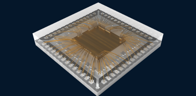
Semiconductor packaging is essential for protecting and interconnecting devices, ensuring reliability and performance. As electronic systems grow more complex, multi-chip packaging has become a key solution, integrating multiple chips into a single package to reduce footprint, enhance electrical performance, and improve thermal management. Among various approaches, leadframe-based designs offer a cost-effective and efficient alternative to substrate-based solutions. The leadframe provides mechanical support and electrical connections while facilitating signal transmission and heat dissipation. This makes it particularly valuable in high-performance and miniaturized electronics. One advanced packaging method leveraging these benefits is Multi-Chip Leadframe, which simplifies manufacturing while maintaining high functionality. As demand for compact, high-performance semiconductor solutions continues to rise, this technology remains a crucial driver of innovation in the industry. 阅读更多
CONTACT US
4th Floor, A3 Building, HuaFeng Industrial Park, GuanTian Village, BeiHuan Road, ShiYan Street, Bao An District, Shenzhen City, Guangdong Province, China
Tel:086 (0)755-8524-1496
WhatsApp: 8615014077679
Skype: Henrychinasz
📧 pcb@alcantapcb.com
CONTACT US
SHIPPING
![]()
CERTIFCATION
![]()
recent articles
 Copper Core PCB vs Aluminium Core PCB Explained2025-09-18 - 7:13 上午
 Microwave PCB Manufacturers | RF Design and Fabrication2025-09-16 - 7:58 上午
 Flex PCB Manufacturing Process: Step-by-Step Guide2025-09-10 - 6:59 上午
 PCB Lamination Process & Sequential Lamination2025-09-04 - 8:10 上午

