
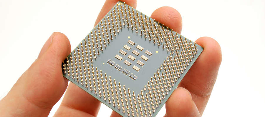
BGA Substrates
Reliable BT substrate solutions with stable circuit structures and customized dimensions for Ball Grid Array packaging applications.
CSP Substrates
Compact BT substrates designed for Chip Scale Packages requiring high-density routing and reduced package dimensions.
SiP Substrates
Customized multilayer BT substrates for System-in-Package modules integrating multiple chips and electronic components.s.
Custom BT Substrates
Application-specific BT substrates with customized thicknesses, layer structures, dimensions and circuit configurations.
BT Substrates for Advanced Electronic Applications
Modern semiconductor packages require substrate materials with reliable thermal, electrical and mechanical performance.
ALCANTA provides custom BT substrate manufacturing based on package structure, circuit density, dimensional requirements and assembly conditions.
✓ Fine-line circuit capability
✓ Customized stack-up design
✓ Stable substrate structures
✓ Engineering and production support
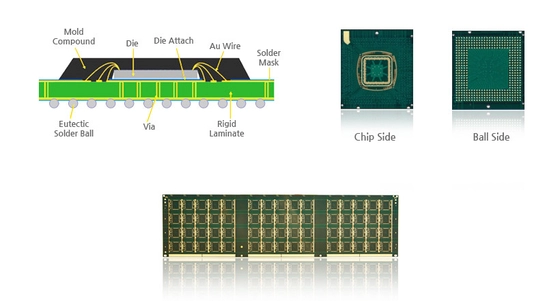
BT Substrate Solutions
Thermal Stability and Packaging Reliability
BT resin substrates provide reliable thermal resistance, electrical insulation and structural stability for semiconductor packaging applications.
Typical Applications:
- BGA Packages
- Memory Packages
- Semiconductor Modules
BT Substrate Manufacturing Capability
| Item | Capability |
|---|---|
| Material | BT Resin Laminate |
| Line / Space | 9 μm / 9 μm |
| Minimum Via Diameter | 55 μm |
| Layer Structure | Customized |
| Board Thickness | Customized |
| Board Size | Customized |
| Circuit Structure | Application-Based |
| Surface Finish | Customized |
| Quality Control | Electrical and Reliability Testing |
Actual manufacturing capability depends on the selected BT material, copper thickness, layer count, substrate thickness, product dimensions and circuit structure.
Final specifications are confirmed after engineering review.
From Design Review to Production
Engineering Review
Material requirements, circuit design, layer structure, dimensions and manufacturing feasibility are evaluated before production.
Prototype Validation
Prototype development and performance validation are provided for customized BT substrate solutions.
Volume Production
Stable manufacturing capability, quality control and continued production support are provided after design validation.
Frequently Asked Questions About BT Substrates
What are BT Substrates?
BT Substrates are package substrates manufactured using Bismaleimide-Triazine resin-based laminate materials.
They provide electrical interconnection and mechanical support between semiconductor chips and external printed circuit boards.
What applications use BT Substrates?
BT Substrates are commonly used in BGA, CSP, SiP, memory packages, semiconductor modules, sensors and compact electronic devices.
What are the advantages of BT Substrates?
BT Substrates provide reliable thermal resistance, electrical insulation, mechanical strength and dimensional stability for semiconductor packaging.
Can ALCANTA provide customized BT Substrates?
Yes. ALCANTA provides customized BT Substrates based on customer requirements, including layer structure, thickness, dimensions, circuit design and surface finish.
What line and space capability does ALCANTA support?
ALCANTA supports line and space structures down to 9 μm / 9 μm for qualified BT substrate designs.
Final capability depends on material selection, copper thickness, layer structure and product dimensions.
What is the minimum via diameter?
Via diameters down to 55 μm can be evaluated for suitable BT substrate designs.
The final specification depends on the via structure, dielectric thickness and plating requirements.
Does ALCANTA support prototype production?
Yes. ALCANTA supports engineering review, prototype validation and volume production for customized BT substrate projects.


