
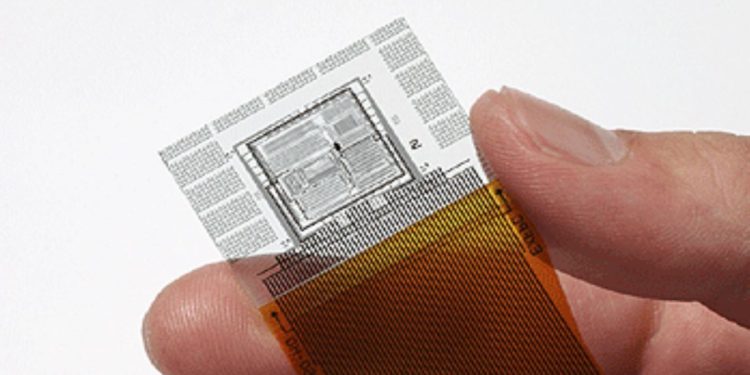
TGV Glass Substrates
Glass substrates with through-glass via structures for vertical electrical interconnection and high-density package integration.
Glass Core Substrates
Rigid and dimensionally stable glass core solutions for advanced package structures and multilayer interconnection.
Metallized Glass Substrates
Custom copper or metal circuit structures formed on glass surfaces for electronic, sensor and optical applications.
Custom Glass Substrates
Application-specific glass substrates with customized thicknesses, dimensions, vias, metallization and circuit patterns.
Glass Substrates for Advanced Electronic Applications
Modern electronic and semiconductor products require stable substrate platforms for precise circuit formation, layer alignment and component integration.
Glass provides a smooth, rigid and electrically insulating base that can support fine circuits, through-glass vias and customized metallization structures.
ALCANTA develops glass substrate solutions according to the mechanical, electrical, optical and assembly requirements of each application.
✓ High dimensional stability
✓ Smooth surface for precise circuit formation
✓ Through-glass via capability
✓ Customized metallization and dimensions
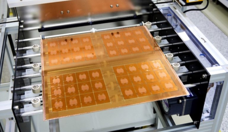
Glass Substrate Solutions
Vertical Interconnection Through Glass
Through-glass vias provide electrical connections between the two sides of a glass substrate and support compact multilayer package structures.
Via dimensions, pitch, aspect ratio and metallization are evaluated according to the selected glass thickness and application.
Typical Applications:
- Advanced Semiconductor Packaging
- Glass Interposers
- Multi-Chip Modules
Glass Substrate Manufacturing Capability
| Base Material | Application-Specific Electronic Glass |
|---|---|
| Minimum Line / Space | Down to 10 μm / 10 μm |
| Minimum Via Diameter | Down to 65 μm |
| Layer Count | 2–16 Layers |
| Maximum Panel Size | Up to 510 × 610 mm |
| Typical Thickness | 0.20–2.00 mm |
| Drilled-Hole Aspect Ratio | Up to 12:1 |
| Via Structure | Through-Glass Vias and Customized Openings |
| Metallization | Customized According to Application |
| Surface Finish | ENIG or Sputtered Gold |
| Substrate Dimensions | Customized |
| Inspection | Dimensional, Electrical and Visual Inspection |
| Production Support | Prototype and Repeat Production |
Actual manufacturing capability depends on glass composition, thickness, panel dimensions, circuit structure, via pitch, metallization and surface-finish requirements.
All final specifications are confirmed through project-specific engineering review.
From Design Review to Production
Engineering Review
We evaluate the glass material, substrate thickness, dimensions, via structure, metallization, circuit design and assembly requirements.
Prototype Validation
Prototype substrates are manufactured and inspected to verify dimensions, circuit formation, vias, metallization and application compatibility.
Repeat Production
Validated products move into controlled repeat or volume production with defined process and inspection requirements.
Frequently Asked Questions About Glass Substrates
What is a glass substrate?
A glass substrate is a thin, flat layer of glass used as a base material for semiconductor devices, particularly in packaging applications. It provides electrical insulation, stability, and support for components like integrated circuits and microchips.
Why are glass substrates used in semiconductor packaging?
Glass substrates are used in semiconductor packaging due to their low dielectric constant, high flatness, low coefficient of thermal expansion (CTE), and excellent thermal stability, making them ideal for high-density interconnects and high-frequency applications.
What are the key benefits of glass substrates over traditional semiconductor substrates?
Glass substrates offer superior thermal stability, low dielectric loss, higher I/O density, and lower warpage, making them more suitable for advanced packaging and high-frequency applications compared to traditional materials like silicon, organic, and ceramic substrates.
What are through-glass vias (TGV)?
Through-glass vias (TGV) are vertical interconnections made through a glass substrate, enabling high-density integration in 3D packaging. TGV technology enhances performance by reducing signal loss and improving thermal dissipation.
How does the low CTE of glass substrates benefit semiconductor packaging?
The low coefficient of thermal expansion (CTE) of glass substrates closely matches that of silicon, reducing thermal stress during heating and cooling cycles, thereby improving the overall reliability and performance of the semiconductor package.
What is the role of Intel’s glass core substrate?
Intel’s glass core substrate provides higher I/O density, improved thermal performance, and reduced warpage for chiplet-based packaging, enabling more efficient and scalable semiconductor solutions for high-performance computing and AI applications.
What are some key players in the glass substrate market?
Key players in the glass substrate industry include Intel, Corning, Absolics, DNP, SKC, and TSMC, which lead the development and manufacturing of high-performance glass substrates for semiconductor applications.
What challenges are faced in mass production of glass substrates?
Challenges include maintaining precision, achieving ultra-thin thicknesses without compromising performance, ensuring uniformity in through-glass via (TGV) creation, and managing the high production costs associated with advanced fine-line patterning techniques.
How do glass substrates contribute to 5G and AI technologies?


