
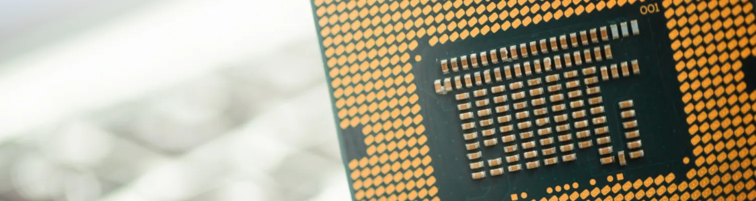
ALCANTA supports customized package substrate development for different semiconductor packaging structures.
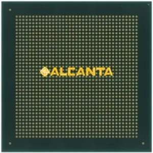
FCBGA Substrate
High-density substrate solutions for flip-chip BGA packages requiring fine-line routing, microvias and multilayer interconnection.
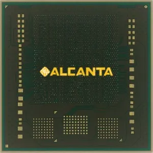
Fine-Pitch BGA Substrate
Fine-feature substrate structures developed for compact semiconductor packages with higher routing density and reduced feature sizes.

IC Package Substrate
Customized package substrate solutions for processors, controllers, communication ICs and other semiconductor devices.
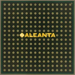
Custom BGA Substrate
Application-specific substrate development based on package dimensions, material systems, layer structures, via configurations and electrical requirements.
BGA Substrate for High-Density Interconnection
A BGA Substrate provides the electrical connection between a semiconductor device and the external printed circuit board.
Its circuit structure redistributes fine-pitch chip connections through multiple routing layers to the solder-ball array on the package side.
For high-density semiconductor packaging, substrate performance depends on the combined control of material, circuit geometry, microvia structure, layer registration and dimensional stability.
ALCANTA provides engineering and manufacturing support based on actual package requirements.
✓ Fine-line circuit capability
✓ Microvia structures
✓ BT and ABF material options
✓ Customized multilayer structures
✓ Prototype and production support

BGA Substrate Solutions
High-Density Circuit Routing
Fine-line structures support increased signal routing density within limited package dimensions.
Suitable for applications requiring compact circuit geometry and high I/O density.
Typical Applications
- FCBGA
- Processor Packages
- High-Density IC Packages
Customer drawings, Gerber data, stack-up information and material specifications can be reviewed before prototype production.
BGA Substrate Manufacturing Capability
| Item | Capability |
| Material | BT, ABF, Customer-Specified Materials |
| Line / Space | Down to 9 μm / 9 μm |
| Minimum Laser Via Diameter | Down to 55 μm |
| Layer Count | 2–26 Layers |
| Layer Structure | Customized |
| Substrate Thickness | 0.10–3.20 mm |
| Maximum Panel Size | Up to 600 × 600 mm |
| Surface Finish | ENIG, ENEPIG, OSP |
| Quality Control | Electrical and Reliability Testing |
Actual manufacturing capability depends on substrate material, copper thickness, dielectric structure, layer configuration, via design and overall package requirements.
Final specifications are confirmed through project-specific engineering review.
From Design Review to Production
Fine-Feature Manufacturing
Fine line / space down to 9 μm / 9 μm and laser via diameters down to 55 μm can be evaluated for suitable designs.
Flexible Material Selection
BT, ABF and customer-specified materials can be reviewed according to package requirements.
Customized Structures
Substrate dimensions, stack-ups, via structures and circuit configurations are developed according to customer designs rather than fixed standard specifications.
Engineering Support
Design files can be reviewed before production to evaluate manufacturability and identify potential process issues.
Prototype to Production
Support is available from initial engineering evaluation and prototype development through repeat production.
Frequently Asked Questions About BGA Substrates
What material can be used for a BGA Substrate?
BT and ABF are common material systems used for semiconductor package substrates.
The appropriate material depends on package structure, circuit density, layer count, electrical performance and reliability requirements.
Customer-specified materials can also be evaluated.
What is the minimum line and space?
Fine line and space down to 9 μm / 9 μm can be evaluated for suitable designs.
Final capability depends on material, copper thickness, dielectric structure and overall substrate configuration.
What is the minimum laser via diameter?
Laser via diameters down to 55 μm can be evaluated depending on material system, dielectric thickness and via structure.
Can you manufacture a custom BGA Substrate?
Yes.
ALCANTA develops customized BGA Substrate structures according to customer drawings, package dimensions, material requirements, stack-up, circuit density and application conditions.
Do you support BT and ABF?
Yes.
Both BT and ABF substrate materials can be evaluated according to the required package architecture and manufacturing specifications.
What are the benefits and limitations of BGA substrates?
BGA substrates offer advantages like improved thermal performance and high-density support but have limitations, such as difficulty in rework and higher production costs.
Can you provide BGA Substrate prototypes? Yes.
Yes.
Prototype development is available for design validation and manufacturing feasibility verification before repeat production.
What files should I provide?
For engineering review and quotation, we recommend providing:
- Gerber or ODB++ files
- Package drawing
- Stack-up
- Material requirement
- Layer count
- Minimum line / space
- Via dimensions
- Copper thickness
- Surface finish
- Prototype or production quantity


