Submit requirements
Share Gerber files, drawings, material preferences and application requirements.


Designed specifically for projects that exceed the capabilities of standard substrates.
01
Material flexibility
Organic, glass, ceramic, metal-based, flexible and high-frequency systems.
02
Complex geometry
Narrow formats, special shapes and non-standard substrate structures.
03
Fine-feature manufacturing
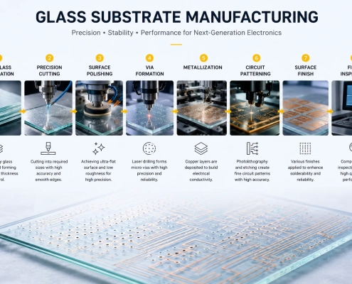
Demonstrated 9/9 μm line/space and 55 μm microvias on applicable designs.
04
Engineering-led evaluation
Every design reviewed around material, stack-up, geometry and performance.
")
Engineered around your design, not a standard catalog.
From established substrate systems to customer-specified materials, every project is evaluated around its material, structure, performance and manufacturing requirements.

Fine-feature organic substrates engineered for high-density interconnect and advanced packaging applications.

Custom glass solutions evaluated around thickness, metallization, via structure and application requirements.

Manufacturing solutions for narrow, elongated, high-aspect-ratio and other non-standard geometries.

FR-4, PI, ceramic, aluminum, copper, PTFE and other project-specific material systems
| Capability | BT / ABF | Glass | Narrow-Format | Multi-Material |
|---|---|---|---|---|
| Minimum Line / Space | 9 / 9 μm | 10 / 10 μm | 9 / 9 μm | 10 / 10 μm |
| Minimum Via Diameter | 55 μm | 65 μm | 55 μm | 65 μm |
| Layer Count | 2–26 Layers | 2–16 Layers | 2–18 Layers | 2–26 Layers |
| Maximum Panel / Length | 600 × 600 mm | 510 × 610 mm | 25 × 1,200 mm | 600 × 610 mm |
| Typical Thickness | 0.10–3.20 mm | 0.20–2.00 mm | 0.10–1.60 mm | 0.20–3.20 mm |
| Drilled-Hole Aspect Ratio | Up to 15:1 | Up to 12:1 | Up to 15:1 | Up to 12:1 |
| Surface Finish Options | ENIG, ENEPIG, OSP | ENIG, Sputtered Au | ENIG, ENEPIG, OSP | ENIG, ENEPIG, Ag |
Capabilities are engineered around material properties, substrate dimensions and application requirements. Contact our engineering team for project-specific capability evaluation.
High-performance substrate solutions across the most demanding industries.

Share Gerber files, drawings, material preferences and application requirements.
We assess material compatibility, geometry, stack-up and key process risks.
Questions, adjustments and critical specifications are aligned with your team.
Samples are manufactured, inspected and documented against agreed requirements.
Validated projects move into repeat or volume production with traceable quality.
 https://pcbmake.com/wp-content/uploads/2026/07/glass-substrate-manufacturing.webp
1024
1536
pcbmake_admin
http://pcbmake.com/wp-content/uploads/2024/02/A去水印-1030x138.png
pcbmake_admin2026-07-23 08:45:282026-07-23 08:45:28Glass Substrate Manufacturing | Process, Materials & Applications
https://pcbmake.com/wp-content/uploads/2026/07/glass-substrate-manufacturing.webp
1024
1536
pcbmake_admin
http://pcbmake.com/wp-content/uploads/2024/02/A去水印-1030x138.png
pcbmake_admin2026-07-23 08:45:282026-07-23 08:45:28Glass Substrate Manufacturing | Process, Materials & Applications https://pcbmake.com/wp-content/uploads/2025/09/copper-core-pcb.webp
394
711
pcbmake_admin
http://pcbmake.com/wp-content/uploads/2024/02/A去水印-1030x138.png
pcbmake_admin2025-09-18 07:13:482025-09-18 07:13:48Copper Core PCB vs Aluminium Core PCB Explained
https://pcbmake.com/wp-content/uploads/2025/09/copper-core-pcb.webp
394
711
pcbmake_admin
http://pcbmake.com/wp-content/uploads/2024/02/A去水印-1030x138.png
pcbmake_admin2025-09-18 07:13:482025-09-18 07:13:48Copper Core PCB vs Aluminium Core PCB Explained https://pcbmake.com/wp-content/uploads/2025/09/microwave-PCB-Manufacturer-1.webp
385
784
pcbmake_admin
http://pcbmake.com/wp-content/uploads/2024/02/A去水印-1030x138.png
pcbmake_admin2025-09-16 07:58:502025-09-18 06:55:23Microwave PCB Manufacturers | RF Design and Fabrication
https://pcbmake.com/wp-content/uploads/2025/09/microwave-PCB-Manufacturer-1.webp
385
784
pcbmake_admin
http://pcbmake.com/wp-content/uploads/2024/02/A去水印-1030x138.png
pcbmake_admin2025-09-16 07:58:502025-09-18 06:55:23Microwave PCB Manufacturers | RF Design and Fabrication https://pcbmake.com/wp-content/uploads/2025/09/flex-pcb-manufacturing-process.webp
1536
1024
pcbmake_admin
http://pcbmake.com/wp-content/uploads/2024/02/A去水印-1030x138.png
pcbmake_admin2025-09-10 06:59:532025-09-10 06:59:53Flex PCB Manufacturing Process: Step-by-Step Guide
https://pcbmake.com/wp-content/uploads/2025/09/flex-pcb-manufacturing-process.webp
1536
1024
pcbmake_admin
http://pcbmake.com/wp-content/uploads/2024/02/A去水印-1030x138.png
pcbmake_admin2025-09-10 06:59:532025-09-10 06:59:53Flex PCB Manufacturing Process: Step-by-Step Guide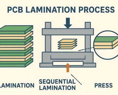 https://pcbmake.com/wp-content/uploads/2025/09/pcb-lamination.webp
1024
1536
pcbmake_admin
http://pcbmake.com/wp-content/uploads/2024/02/A去水印-1030x138.png
pcbmake_admin2025-09-04 08:10:082025-09-04 08:12:24PCB Lamination Process & Sequential Lamination
https://pcbmake.com/wp-content/uploads/2025/09/pcb-lamination.webp
1024
1536
pcbmake_admin
http://pcbmake.com/wp-content/uploads/2024/02/A去水印-1030x138.png
pcbmake_admin2025-09-04 08:10:082025-09-04 08:12:24PCB Lamination Process & Sequential Lamination https://pcbmake.com/wp-content/uploads/2025/08/ptfe-pcb.webp
426
711
pcbmake_admin
http://pcbmake.com/wp-content/uploads/2024/02/A去水印-1030x138.png
pcbmake_admin2025-08-28 09:16:442025-08-28 09:20:46PTFE PCB: Cost, Rogers vs FR4 & Polyimide
https://pcbmake.com/wp-content/uploads/2025/08/ptfe-pcb.webp
426
711
pcbmake_admin
http://pcbmake.com/wp-content/uploads/2024/02/A去水印-1030x138.png
pcbmake_admin2025-08-28 09:16:442025-08-28 09:20:46PTFE PCB: Cost, Rogers vs FR4 & Polyimide https://pcbmake.com/wp-content/uploads/2025/08/pcb-board-designer.webp
415
899
pcbmake_admin
http://pcbmake.com/wp-content/uploads/2024/02/A去水印-1030x138.png
pcbmake_admin2025-08-27 06:37:372025-08-27 06:37:37How to Test a PCB: Methods, Equipment, and Multimeter Guide
https://pcbmake.com/wp-content/uploads/2025/08/pcb-board-designer.webp
415
899
pcbmake_admin
http://pcbmake.com/wp-content/uploads/2024/02/A去水印-1030x138.png
pcbmake_admin2025-08-27 06:37:372025-08-27 06:37:37How to Test a PCB: Methods, Equipment, and Multimeter Guide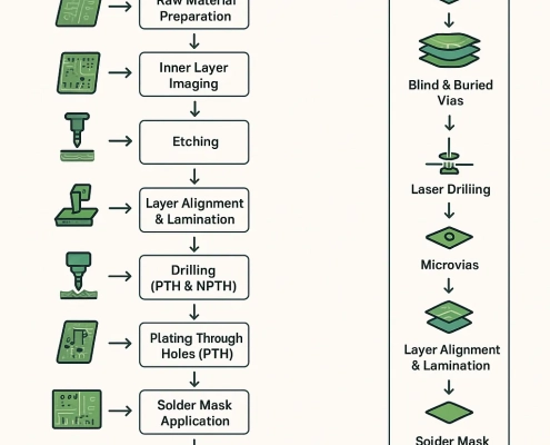 https://pcbmake.com/wp-content/uploads/2025/08/pcb-manufacturing-process.webp
1536
1024
pcbmake_admin
http://pcbmake.com/wp-content/uploads/2024/02/A去水印-1030x138.png
pcbmake_admin2025-08-22 07:12:092025-08-22 07:14:17PCB Manufacturing Process: Step-by-Step Guide
https://pcbmake.com/wp-content/uploads/2025/08/pcb-manufacturing-process.webp
1536
1024
pcbmake_admin
http://pcbmake.com/wp-content/uploads/2024/02/A去水印-1030x138.png
pcbmake_admin2025-08-22 07:12:092025-08-22 07:14:17PCB Manufacturing Process: Step-by-Step Guide https://pcbmake.com/wp-content/uploads/2025/08/PTH-PCB.webp
1024
1536
pcbmake_admin
http://pcbmake.com/wp-content/uploads/2024/02/A去水印-1030x138.png
pcbmake_admin2025-08-19 07:54:002025-08-19 07:54:00PTH PCB Guide: Design, NPTH vs PTH, Vias & Components
https://pcbmake.com/wp-content/uploads/2025/08/PTH-PCB.webp
1024
1536
pcbmake_admin
http://pcbmake.com/wp-content/uploads/2024/02/A去水印-1030x138.png
pcbmake_admin2025-08-19 07:54:002025-08-19 07:54:00PTH PCB Guide: Design, NPTH vs PTH, Vias & ComponentsTell us your material, structure, dimensions and application requirements. Our engineering team will help identify a manufacturable solution.
Our factory has implemented lean improvements in areas like DFM, NPI, IQC, IPQC, and OQA. These efforts have helped us achieve certifications including ISO 9001:2015, ISO 13485, IATF 16949, and SGS. Our dedication to quality and service has built long-term relationships with medium and large customers.

Tell us your material, structure and application requirements. Our engineering team will help identify the right solution.
SHIPPING
![]()
CERTIFCATION
![]()