
Essential Guide to Designing a Flexible PCB Prototype
A flexible pcb prototype is an early-stage version of a flexible printed circuit board used for design validation before full-scale production. Unlike traditional rigid PCBs, flexible PCBs can bend, fold, and conform to complex shapes, making them ideal for modern compact and lightweight electronic devices. The flexible pcb prototype allows engineers to test mechanical and electrical performance under real-world conditions, reducing development risk and cost.
In today’s electronics industry, the demand for flexibility, durability, and space efficiency continues to grow. As a result, flexible printed circuit boards play a critical role in the rapid development and advancement of smart technology.
Typical applications include wearables, such as fitness trackers and smartwatches, medical devices like portable monitors, mobile electronics including foldable phones and tablets, and high-performance systems in aerospace and automotive sectors, where reliability and flexibility are essential. These flexible circuits enable engineers to bring advanced designs to life quickly and efficiently.
Basic Structure and Types of Flexible PCBs for flexible pcb prototype
A flexible pcb prototype begins with selecting the right base materials. The most common substrates are polyimide— prized for its excellent thermal stability and chemical resistance— and PET (polyethylene terephthalate), which offers lower cost and moderate flexibility. Polyimide substrates can withstand higher temperatures (up to 260 °C) and provide superior mechanical endurance for dynamic bending, while PET is suitable for applications with less demanding thermal requirements.
Flexible PCBs are available in three main configurations:
-
Single-sided flex PCBs feature copper circuitry on one side of the substrate and are ideal for simple, low-density interconnects.
-
Double-sided flex PCBs have conductive traces on both sides, with through-holes or plated vias providing interlayer connections, enabling more complex routing in a compact form factor.
-
Multilayer flex PCBs stack alternating layers of copper and dielectric films (polyimide or PET), allowing very high wiring density for advanced designs.
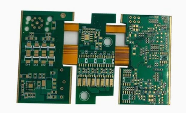
Rigid-flex PCBs combine rigid FR-4 sections with flexible interconnects in a single assembly. Unlike pure flex, rigid-flex boards offer the structural support of rigid boards and the space-saving advantages of flex circuits, making them perfect for three-dimensional and space-constrained designs.
Key Design Considerations for flexible pcb prototype
When designing a flexible pcb prototype, engineers must adhere to a set of rigorous guidelines to ensure performance and reliability:
Design Rules for a Flexible PCB Prototype
-
Bend Radius: Maintain a minimum bend radius of at least ten times the total flex stack thickness to prevent conductor fatigue and cracking.
-
Trace Width and Spacing: Calculate trace widths based on current-carrying requirements and account for the thinner copper foil used in flex. Ensure adequate spacing to avoid shorting during flexing.
-
Pad and Component Layout: Place components off the bend areas whenever possible. Use teardrop or filleted pads near holes and bends to reduce stress concentrations.
Reliability and Thermal Management in flexible pcb prototype Design
-
Coverlay Selection: Choose appropriate polyimide coverlays or films that protect copper traces and provide insulation without compromising flexibility.
-
Heat Dissipation: Design heat-sinking areas or integrate stiffeners where high-power components are mounted. Ensure thermal vias or copper planes are placed to spread heat efficiently.
Signal Integrity and EMI Issues in flexible pcb prototype
-
Controlled Impedance: For high-speed signals, define and simulate trace stackups to achieve consistent impedance.
-
EMI Mitigation: Incorporate ground planes, shielding layers, or flex-compatible ferrite beads to minimize electromagnetic emissions and susceptibility.
Supported CAD Tools for Flexible PCB Prototype Design
-
Altium Designer: Offers native flex and rigid-flex stackup management with real-time DFM checks.
-
KiCad: An open-source option with flex-specific layer definitions and bend line annotations.
-
Eagle: Provides basic flex stackup support and user-defined layer sets for simple prototypes.
Adhering to these considerations early in the CAD phase will streamline fabrication, reduce risk, and ensure a successful flexible PCB prototype run.
Manufacturing Process Overview for flexible pcb prototype
The fabrication of a flexible pcb prototype involves precise, multilayered processes tailored to achieve both electrical performance and mechanical flexibility. Understanding each step in the manufacturing cycle is critical for optimizing turnaround time and ensuring design accuracy.
Main Steps in Fabrication
-
Copper Cladding: A thin copper foil is laminated onto a flexible substrate such as polyimide using adhesives or adhesiveless bonding techniques.
-
Etching: Photolithography is used to define circuit patterns, followed by chemical etching to remove unwanted copper and form the traces.
-
Drilling: Micro-drilling or laser drilling creates vias and holes for interconnections between layers or component mounting.
-
Coverlay Application: A flexible polyimide film, known as a coverlay, is laminated over the etched circuits to protect them from environmental exposure and provide insulation.
-
Testing: Electrical testing ensures continuity and absence of shorts, which is vital for any flexible pcb prototype before further integration.
Prototype vs. Mass Production
The main difference between a flexible pcb prototype and a production unit lies in speed and customization. Prototypes are typically manufactured in smaller batches using quick-turn processes, with a focus on design validation. Mass production emphasizes cost-efficiency, scalability, and tighter process control. Material sourcing, tooling, and panel optimization are streamlined in production, whereas prototypes allow greater flexibility for revisions.
Surface Finishes
Surface treatments ensure solderability and long-term reliability. Common finishes include:
-
ENIG (Electroless Nickel Immersion Gold): Offers excellent flatness and oxidation resistance, suitable for fine-pitch components.
-
OSP (Organic Solderability Preservative): A cost-effective and environmentally friendly option, ideal for short-term prototype builds.
Laser Cutting vs. Mechanical Methods
For outline shaping and internal cutouts, laser cutting is preferred in manufacturing flexible PCBs due to its precision and non-contact processing, which minimizes mechanical stress. Mechanical routing may be used in production when cost and throughput are more critical.
A deep understanding of these processes ensures a more predictable, higher-quality prototype, ultimately bridging the gap between concept and mass production.
Leading flexible pcb prototype Manufacturers (from provided links)
Choosing the right manufacturing partner is critical to the success of any flexible pcb prototype project. A reliable supplier ensures high-quality production, short lead times, and design flexibility during the prototyping phase. Below are several top manufacturers offering specialized services for flexible PCB prototypes, based on the provided references.
PCBWay
PCBWay Flex PCB Page
PCBWay is a popular choice for designers seeking a flexible pcb prototype with fast turnaround and extensive customization options. They support single- to multi-layer flexible PCBs and provide custom stackup configurations, ideal for unique design needs. Their online quote system is user-friendly, and their global reputation is built on competitive pricing and consistent quality.
Epec
Epec Prototypes
Epec specializes in high-reliability flexible and rigid-flex PCB manufacturing. Their flexible pcb prototype service emphasizes durability and performance, making them a strong choice for aerospace, defense, and medical industries. Epec’s engineering team also provides in-depth support during the design and DFM (Design for Manufacturability) stages.
Technotronix
Technotronix Flex PCB
Technotronix is known for its quick-turn manufacturing capabilities, particularly in custom flexible pcb prototype solutions. They accommodate complex layouts and offer support for HDI, impedance control, and multilayer flex designs. Their rapid prototyping services are especially valuable to startups and development teams needing accelerated iteration.
Other Notable Providers
-
ProtoExpress (Sierra Circuits)
Offers comprehensive flex and rigid-flex PCB services with a focus on engineering-driven design support and quick prototyping. -
PCBGoGo
Known for budget-friendly flexible pcb prototype services with fast lead times, suitable for hobbyists and commercial R&D. -
Hemeixin
Provides a full spectrum of advanced flex PCB solutions including microvias, embedded components, and rigid-flex hybrids. They emphasize tight tolerances and high-density layouts. -
FlexPCB.com
A dedicated flex circuit manufacturer with decades of experience in producing both simple and complex flexible pcb prototype designs. They offer design consultation and support for demanding industrial applications.
Each of these manufacturers brings unique strengths, and selecting the right one depends on your project’s complexity, lead time, and budget.
Stackup Example and Analysis for flexible pcb prototype
The layer stackup is a foundational element in the design of any flexible pcb prototype, as it directly impacts the circuit’s mechanical flexibility, electrical performance, and manufacturability. Selecting the right stackup is especially important in early prototyping stages to ensure accurate testing and downstream production compatibility.
Sample Stackups from PCBWay
PCBWay provides several standard and customizable stackup options for flexible pcb prototype orders. A typical single-layer stackup consists of:
-
Polyimide base substrate
-
Copper foil
-
Adhesive (optional)
-
Coverlay film
For double-layer flexible PCBs, the stackup might include:
-
Coverlay
-
Top copper
-
Polyimide dielectric
-
Bottom copper
-
Bottom coverlay
Multilayer flexible PCBs integrate alternating layers of copper and dielectric film, often incorporating adhesive layers and polyimide stiffeners in areas that require extra rigidity.
Choosing the Right Layer Structure for Your Prototype
When designing a flexible pcb prototype, consider the following when choosing your stackup:
-
Mechanical Flexibility: Fewer layers and thinner materials offer better bendability. For dynamic applications (e.g., wearable tech), single or double layers are preferred.
-
Signal Routing and Grounding: Multilayer structures are ideal when more signal integrity and ground shielding are needed, especially in high-speed circuits.
-
Component Density: If your design demands compact, complex routing, opt for a 3- to 4-layer stackup, which allows finer trace geometry and better EMI control.
-
Thermal Considerations: Thicker copper and multiple planes may be needed for power handling and heat dissipation.
Comparison with Rigid-Flex Stackups
Unlike a pure flexible PCB, a rigid-flex stackup combines both rigid FR-4 sections and flexible polyimide regions in a single board. This configuration is ideal for 3D assemblies where components are mounted on rigid zones while flexible zones handle movement and interconnection. While more complex and expensive, rigid-flex offers structural support and space efficiency in compact designs such as foldable phones or aerospace instruments.
Choosing between a flexible and rigid-flex design depends on your product’s mechanical, thermal, and electrical needs. PCBWay and other top manufacturers offer design consultation to help tailor the most efficient stackup.
Common Challenges & Solutions for flexible pcb prototype
Building a flexible pcb prototype often reveals specific manufacturing and design challenges. Recognizing these issues early helps you mitigate risk and improve yield.
Frequent Issues
-
Cracking: Repeated bending or overly tight bend radii can fracture copper traces. Solution: Increase the minimum bend radius and reinforce high-stress areas with polyimide stiffeners.
-
Delamination: Poor adhesion between copper and substrate leads to layer separation. Solution: Specify adhesiveless copper and use high-quality coverlay laminates to enhance bonding.
-
Routing Problems: Complex trace patterns on thin substrates can cause alignment errors or impedance mismatches. Solution: Simplify critical signal routes, maintain uniform trace width, and verify against manufacturer DFM guidelines.
Quality Control Tips
-
Incoming Inspection: Request optical and electrical tests (AOI, flying probe) on your flexible pcb prototype to catch defects before assembly.
-
Pilot Runs: Order a small batch to validate your design and manufacturing process, allowing adjustments without high cost.
Reducing Turnaround Time
-
Standard Specs: Use common material thicknesses, copper weights, and layer counts supported by your manufacturer to avoid special tooling delays.
-
Panelization: Combine multiple layouts on a single panel with shared tooling features to speed up processing and reduce handling.
By proactively addressing these challenges, you can accelerate development and achieve a robust prototype.
Cost and Lead Time Breakdown for flexible pcb prototype
Understanding the cost structure and delivery timeline of a flexible pcb prototype is essential for effective project planning and budget control. Pricing and lead time vary significantly based on complexity, quantity, and vendor capabilities.
Typical Pricing Models by Different Manufacturers
Manufacturers such as PCBWay, Epec, and Technotronix typically offer one of the following pricing structures for a flexible pcb prototype:
-
Flat-rate prototyping: Ideal for small quantities with fixed specifications (e.g., single- or double-layer). This model is commonly offered by PCBWay, where costs can start as low as $80–$150 depending on size and complexity.
-
Custom quote model: Used for multilayer or rigid-flex designs requiring unique stackups, special materials, or tight tolerances. Companies like Epec and FlexPCB.com offer detailed quotes based on DFM analysis.
-
Online calculators: Sites such as ProtoExpress and PCBGoGo allow instant pricing estimates based on layer count, board size, and turnaround time.
Cost Difference: Prototype vs Production
A flexible pcb prototype is significantly more expensive on a per-unit basis than mass production. Reasons include:
-
Low volume: Tooling and setup costs are distributed over fewer units.
-
Faster turnaround: Expedited processing and premium materials raise costs.
-
Customization: Prototypes often use non-standard stackups or materials, increasing production complexity.
For example, a single flexible pcb prototype might cost $200–$500, whereas the same board could drop to $10–$20 per unit in a 1,000+ production run due to economies of scale.
Key Factors That Affect Delivery Time
-
Layer count and complexity: Multilayer and rigid-flex prototypes typically take longer (7–15 days) versus single-layer designs (3–5 days).
-
Material availability: Custom materials or copper weights may delay production. Choosing standard specs helps speed up processing.
-
DFM approval: Delays in finalizing the design or resolving DFM issues can add days. Always communicate proactively with your manufacturer.
-
Panelization and tooling: Proper panelization can reduce fabrication and assembly time, especially for multi-board projects.
By selecting the right manufacturer and optimizing your design for manufacturability, you can minimize both cost and lead time for your flexible pcb prototype while maintaining quality.
Trends and Future Outlook for flexible pcb prototype
The evolution of electronic technology continues to drive demand for advanced flexible pcb prototype solutions that can meet the stringent requirements of emerging applications. As 5G, IoT, and smart devices become ubiquitous, flexible PCBs are playing an increasingly vital role in enabling compact, high-performance designs.
Role of Flexible PCBs in 5G, IoT, and Smart Devices
The rollout of 5G networks demands antennas and RF modules that are lightweight, compact, and capable of withstanding mechanical stress. Flexible PCBs provide the perfect platform for these components by supporting complex signal routing while conforming to small, irregular spaces. Similarly, IoT devices and wearables require durable, bendable circuits for seamless integration into clothing, accessories, or medical equipment. This type of prototype allows engineers to validate new designs that combine flexibility with robust electrical performance in these rapidly growing markets.
Hybrid Designs: Flex + Rigid + Modular
Future product designs increasingly utilize hybrid approaches, combining flexible, rigid, and modular PCB sections. This allows designers to optimize each area for specific needs—flexible sections for movement and space savings, rigid sections for component mounting and mechanical strength, and modular parts for easy upgrading or repair. Prototyping such complex assemblies requires sophisticated flexible pcb prototype services that can handle multi-material stackups and intricate interconnections.
HDI Flex PCB Trends (High Density Interconnects)
As devices shrink and demand faster data rates, HDI flex PCBs are becoming the standard for advanced electronics. These boards feature microvias, finer traces, and multiple layers in a compact form factor. Developing an HDI flex PCB requires precision manufacturing and stringent quality controls but offers significant performance advantages. HDI flex is especially important in applications like smartphones, aerospace electronics, and high-speed computing.
The future of the flexible pcb prototype market is bright, driven by innovations in material science, manufacturing techniques, and ever-increasing demands for miniaturized, multifunctional devices. Staying updated on these trends ensures your designs remain competitive and forward-looking.

