
Key Factors Influencing Flexible PCB Thickness Choices
Flexible PCBs, also known as flex circuits, are lightweight, bendable electronic interconnects used across a wide range of applications such as wearable technology, medical devices, automotive systems, and aerospace electronics. These circuits allow designers to save space, reduce weight, and improve mechanical flexibility in compact or moving products. One of the most critical design parameters in flex circuit development is flexible PCB thickness. This factor significantly influences the circuit’s ability to bend without damage, carry current effectively, and fit within mechanical enclosures. Whether a design requires extreme flexibility for dynamic applications or added stiffness for stable routing, PCB thickness must be carefully selected to meet both electrical and mechanical requirements. This article provides an in-depth look into how to evaluate, choose, and optimize board thickness for various use cases. By understanding these principles, designers and engineers can make more informed decisions when developing reliable, high-performance flexible electronic solutions.
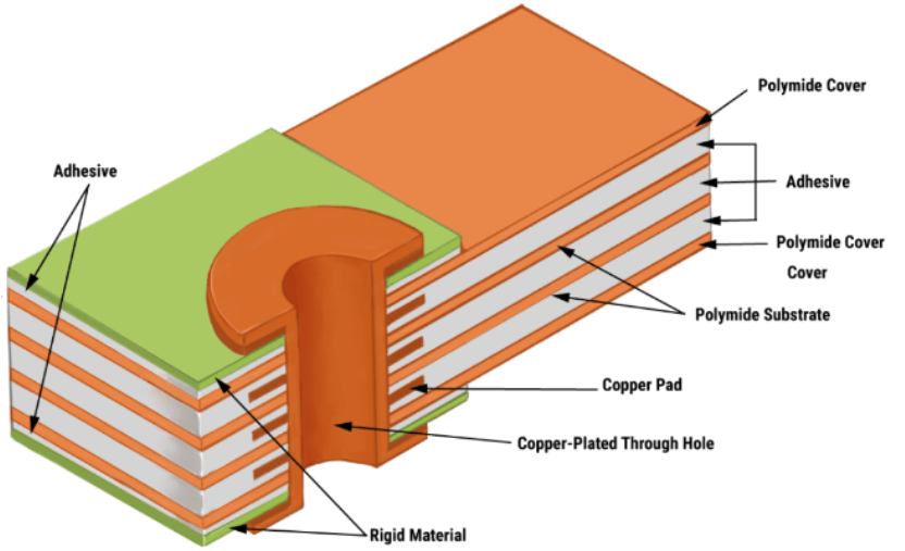
Basic Structure of a Flexible PCB and the Role of Flexible PCB Thickness
A clear understanding of the layered construction is essential when selecting flexible PCB thickness, as each material directly contributes to overall board rigidity, bend radius, and electrical performance.
Copper Foil (Conductor Layer)
The copper foil provides the electrical pathways. Standard weights range from 0.5 oz to 2 oz; heavier copper increases current-carrying capacity but adds to total thickness. A 1 oz foil (≈35 µm) is common for balanced flexibility and conductivity.
Polyimide (PI) Substrate
Polyimide serves as the base dielectric. Film thicknesses typically are 12.5 µm, 25 µm, or 50 µm. Thinner PI enables tighter bend radii, while thicker PI improves dimensional stability. The substrate dominates the flex region’s thickness budget.
Adhesive or Adhesiveless Layers
Adhesive-based constructions bond copper to PI with an acrylic or epoxy layer (~10–20 µm), adding to thickness and potentially reducing flexibility. Adhesiveless (direct copper-to-PI) designs minimize adhesive thickness, yielding slimmer, more reliable flex circuits.
Coverlay or Solder Mask
A coverlay of PI (25–50 µm) or a flexible solder mask protects conductors from moisture and abrasion. Coverlays increase mechanical protection but contribute additional microns to the stack-up.
Optional Layers
- Stiffeners: Rigid inserts (PI, FR-4, or stainless steel) locally reinforce areas for connector support, with typical thicknesses from 0.2 mm to 1.6 mm.
- Shielding Layers: Overlaid metal or foil shields for EMI control can add another 50–75 µm.
By carefully balancing these materials, designers can optimize flexible PCB thickness to meet both mechanical and electrical requirements without overbuilding the flex sections.
Common Ranges for Flexible PCB Thickness
Understanding typical flexible PCB thickness ranges helps designers balance flexibility, strength, and manufacturability. Below are the most common categories:
Standard Flexible PCB Thickness Values for Common Applications
Single and double-layer flex circuits typically span a total thickness of 0.05 mm to 0.30 mm. Within this range:
- Copper weights: 0.5 oz (≈17 µm), 1 oz (≈35 µm), and 2 oz (≈70 µm). Higher copper weights improve current capacity but increase flexible PCB thickness and reduce bendability.
- Polyimide (PI) film thickness: Common values are 12.5 µm, 25 µm, and 50 µm (0.5 mil to 2 mil). Thinner PI films offer a smaller flex neutral axis and tighter bend radii, while thicker films add durability at the cost of added thickness.
Multilayer Flexible PCBs and Their Impact on Flexible PCB Thickness
Every additional copper/PI layer and adhesive adds to the stack-up, causing total thickness to exceed 0.5 mm in complex designs. To preserve flexibility, engineers may:
- Use adhesiveless constructions to eliminate adhesive layers.
- Limit layer count in high-flex regions and reserve multilayer stacks for static zones.
Flexible PCB Thickness Tolerance and Minimum Limits
Fabricators set both standard and custom minima based on process capabilities:
- JLCPCB offers standard flex cores from 0.15 mm to 0.30 mm, with custom options down to 0.10 mm.
- Hemeixin supports a minimum of 0.05 mm in single-layer, adhesive-less builds.
- NCAB typically specifies 0.10 mm as the lower limit but can accommodate 0.08 mm in advanced processes.
Always verify your manufacturer’s flexible PCB thickness tolerances and capabilities before finalizing the design.
Key Factors Affecting Flexible PCB Thickness
Selecting the appropriate thickness for a flexible PCB involves careful evaluation of electrical, mechanical, and manufacturing factors. Each aspect directly impacts the board’s performance, reliability, and cost. Below are the primary considerations influencing design decisions.
Electrical Requirements
Electrical performance plays a key role in determining the necessary copper thickness, which directly contributes to flexible PCB thickness:
-
Current carrying capacity depends on copper weight. Heavier copper (e.g., 2 oz) supports higher currents but significantly increases thickness and stiffness.
-
Signal integrity and impedance control are essential in high-speed or RF designs. Controlled impedance often requires specific dielectric thicknesses and spacing between layers, affecting the total stack height.
-
EMI shielding requirements may introduce additional copper or conductive layers, adding both electrical protection and physical thickness.
Mechanical and Flexibility Considerations
Mechanical constraints are especially critical in dynamic or tight-space applications:
-
Thinner = more flexible, but often less durable under repeated bending.
-
Bend radius rules recommend a minimum bend radius of 10x the total flexible PCB thickness for dynamic applications.
-
Static vs dynamic flex designs require different thickness strategies—dynamic flex regions typically use minimal copper and thinnest PI to enhance lifespan.
Layer Count and Stack-Up Design
As more layers are added, total flexible PCB thickness naturally increases:
-
Multilayer flex circuits require additional dielectric and copper layers, increasing rigidity and bend radius.
-
Adhesiveless constructions help reduce thickness by eliminating adhesive layers between copper and PI, improving both flexibility and reliability.
Manufacturing Constraints
Fabrication capabilities vary across PCB suppliers, affecting the minimum and maximum supported flexible PCB thickness:
-
JLCPCB offers flex cores starting from 0.15 mm, with tighter control available through custom stack-ups.
-
Hemeixin and PCBWay provide ultra-thin options down to 0.05 mm for high-flex or wearable applications.
-
Advanced fabs like Epec support controlled impedance and fine-pitch designs while managing tight thickness tolerances.
Designers must work closely with manufacturers to align design expectations with real-world production limits for flexible PCB thickness.
Thickness Considerations in Rigid-Flex PCBs and Flexible PCB Thickness
When designing rigid-flex circuits, managing flexible PCB thickness across both rigid and bendable zones is crucial to ensure reliability and performance.
Thickness Difference Between Rigid and Flex Sections
Rigid areas (typically FR-4) often range from 0.8 mm to 1.6 mm to support connectors and heavy components, while flex regions are designed as thin as 0.10 mm to 0.30 mm. This contrast in flexible PCB thickness enables stiff mounting zones alongside highly conformable sections.
Importance of Stiffeners and Their Impact on Overall Thickness
Stiffeners (made from PI, FR-4, or stainless steel) are added to flex areas that need component support or connector reinforcement. A typical PI stiffener adds 0.2 mm to 0.3 mm locally, enhancing mechanical stability without compromising the bend zone’s minimum thickness.
NCAB and Epec Recommendations for Rigid-Flex Stack-Ups
- NCAB suggests a stack-up with a 0.15 mm flex core, 1 oz copper, and selective stiffening to reach ~0.8 mm in rigid zones, maintaining ≤0.25 mm in flex regions.
- Epec advises using adhesiveless flex cores of 25 µm PI with 0.5 oz copper for dynamic bends, supplemented by 0.3 mm FR-4 stiffeners for static mounting, balancing flexible PCB thickness and mechanical strength.
By carefully specifying the differential thickness and appropriate stiffener placement, engineers can create reliable rigid-flex designs that meet both electrical and mechanical demands.
Industry Standards and Design Recommendations for Flexible PCB Thickness
To ensure performance, safety, and manufacturability, the design of flexible PCB thickness must adhere to industry standards and application-specific guidelines. These standards help engineers define reliable stack-ups and avoid common pitfalls in high-flex or mission-critical applications.
Referencing IPC-2223C and Similar Guidelines
The IPC-2223C standard, published by IPC (Association Connecting Electronics Industries), is the most widely used design guideline for flexible and rigid-flex printed circuit boards. It outlines:
-
Recommended material types and minimum thicknesses
-
Bend radius limitations based on flexible PCB thickness
-
Stack-up configurations for both single-layer and multilayer flexible circuits
Following IPC-2223C helps designers maintain electrical integrity and mechanical durability, especially in dynamic flexing environments.
Recommended Thicknesses by Application
Different applications call for tailored flexible PCB thickness values:
-
Wearables: Ultra-thin constructions of 0.05–0.15 mm are common to maximize comfort and bendability.
-
Medical devices: Require reliable yet compact designs, often in the 0.10–0.20 mm range, with biocompatible materials.
-
Defense and aerospace: Tend to favor thicker flex circuits (0.20–0.30 mm or more) to enhance durability, EMI shielding, and multilayer capabilities under extreme environments.
Examples from ProtoExpress, Epec, and RayPCB
-
ProtoExpress recommends using a 0.12 mm total flexible PCB thickness for one- or two-layer dynamic flex circuits and increasing to 0.25 mm or more for static or semi-rigid zones.
-
Epec offers design kits that include suggested thicknesses for different copper weights and polyimide films, typically ranging from 0.10 mm to 0.30 mm depending on the flex zone’s requirements.
-
RayPCB notes that 0.15 mm is a practical lower limit for most consumer applications, balancing flexibility with manufacturability.
By following these industry-backed recommendations, designers can select optimal thickness values that align with their product’s reliability, functionality, and form factor needs.
How to Choose the Right Flexible PCB Thickness
Selecting the right flexible PCB thickness is a critical step in ensuring both the functionality and reliability of your final product. A systematic approach allows designers to balance performance, flexibility, and manufacturability. Below is a step-by-step process to help guide this decision:
Define Mechanical and Electrical Requirements
Start by clearly outlining the mechanical constraints of your product. Consider:
-
How much the board needs to bend or fold
-
Minimum bend radius allowed
-
Available space within the enclosure
Electrically, determine current requirements (which affect copper thickness), need for impedance control, and EMI shielding. These factors directly impact the overall flexible PCB thickness.
Determine Number of Layers and Flexibility Goals
Choose the minimum number of layers required to meet circuit complexity and routing needs. Fewer layers generally mean a thinner and more flexible PCB. If dynamic flexing is involved, aim for single or double-layer constructions with thin polyimide cores to minimize flexible PCB thickness and reduce mechanical fatigue.
Consult with Manufacturers Early
Engage PCB manufacturers like JLCPCB, Hemeixin, or Epec during the design phase to understand their specific material options, minimum supported thickness, and stack-up recommendations. Early consultation can prevent design iterations and ensure that your chosen specifications are both manufacturable and cost-effective.
Prototype and Validate with Final Assembly
Build physical prototypes using the selected material stack-up and test them in your actual product enclosure. Evaluate bending performance, assembly tolerances, and environmental durability. Adjust the design based on test feedback before scaling to mass production.
By following this structured approach, engineers can confidently select the right thickness to meet their application’s mechanical, electrical, and commercial demands.

