
Essential Guide to QFN Package Size: PCB Layout Tips

QFN (Quad Flat No-Lead) packages are a popular choice in modern electronic designs, offering compact size, high performance, and cost efficiency. The QFN Package Size plays a critical role in determining its functionality, particularly in applications requiring space-saving solutions. This leadless package features a flat, exposed pad design for effective heat dissipation and grounding, making it ideal for high-density circuits. The variety of QFN Package Sizes, such as 3×3 mm or 7×7 mm, allows engineers to tailor the choice to specific requirements like power management and signal integrity. Understanding the dimensions, pad layout, and manufacturing considerations is essential to maximize the package’s potential in consumer electronics, automotive systems, and IoT devices.
Understanding QFN Package Size and Features
The QFN (Quad Flat No-Lead) package is a surface-mount technology widely used in modern electronics for its compact and efficient design. This type of package has no extending leads; instead, it uses flat metal pads at the bottom for electrical connections. Its design includes an exposed thermal pad, which significantly enhances heat dissipation and ensures reliable grounding, making it ideal for high-performance and high-frequency applications.
A critical factor in its adoption is the QFN Package Size, which comes in various dimensions, such as 3×3 mm and 5×5 mm, catering to space-constrained designs. Its compact size reduces PCB footprint, while its low inductance minimizes signal distortion, making it suitable for applications in consumer electronics, automotive systems, and IoT devices.
Get a Quotation ForQFN Package Size Now
QFN Package Size, Structure, and Types
QFN Basic Structure
QFN (Quad Flat No-Lead) packages are designed with a flat, leadless configuration, where electrical connections are made through metal pads on the underside of the package. This eliminates protruding pins, reducing the footprint and improving mechanical stability. One of the key features of this design is the exposed thermal pad at the bottom of the package. This pad provides excellent heat dissipation by directly contacting the PCB, making it ideal for thermally demanding applications. Additionally, the exposed pad enhances grounding, improving electrical performance in high-frequency circuits.
The compact QFN Package Size further optimizes board space, enabling its use in miniaturized devices like smartphones, wearables, and automotive electronics.
Types of QFN Packages
QFN packages are available in several variations to meet diverse design needs:
-
Single-row QFN
- Features a single row of metal pads around the periphery.
- Commonly used in applications where smaller QFN Package Sizes are sufficient.
-
Dual-row QFN
- Adds a second row of pads inside the first row, increasing the number of connections within the same footprint.
- Suitable for designs requiring higher pin counts without compromising size.
-
Examples of Variations
- DFN (Dual Flat No-Lead): A simpler version of QFN with fewer pins, often used for basic analog or power management ICs.
- MLF (Micro Leadframe Package): Offers enhanced thermal and electrical performance, ideal for high-power applications.
Understanding the structure and types of QFN packages ensures optimal selection for designs requiring efficient space utilization, thermal performance, and electrical connectivity.
Get a Quotation ForQFN Package Size Now
Understanding QFN Package Size and Dimensions
The QFN Package Size is a crucial consideration in designing compact and efficient electronic circuits. Its dimensions influence the overall PCB footprint, thermal performance, and electrical connectivity, making it essential to choose the right size for your application.
Standard QFN Dimensions
QFN packages are available in a variety of standard sizes, allowing engineers to select options tailored to specific requirements:
- 3×3 mm: Ideal for compact devices like wearables and IoT sensors, where space-saving is critical.
- 5×5 mm: A versatile size used in consumer electronics and industrial systems for moderate power and pin count requirements.
- 7×7 mm: Suitable for applications requiring higher pin counts or improved thermal performance, such as automotive control systems and high-frequency modules.
These sizes enable engineers to balance space constraints and functionality effectively while optimizing the layout for performance.
Pad and Pitch Details
QFN packages feature a grid of metal pads under the package for electrical connections. The pitch, or the distance between the centers of adjacent pads, typically ranges from 0.4 mm to 0.5 mm, depending on the package size.
Proper pad design is critical for successful PCB integration:
- Accurate pad alignment ensures reliable solder joints and prevents defects such as bridging or voiding.
- Thermal pad considerations: The exposed thermal pad must align with a corresponding PCB pad to enable efficient heat dissipation.
The QFN Package Size directly influences pad layout complexity, requiring precise PCB design to maintain electrical performance and mechanical reliability. By adhering to recommended guidelines, designers can achieve robust connections and optimal package functionality.
Get a Quotation ForQFN Package Size Now
How to Choose the Right QFN Package Size
Choosing the right QFN Package Size is a crucial step in the PCB design process, as it directly impacts performance, cost, and manufacturability. Engineers must consider several factors to ensure the selected size aligns with the requirements of the specific application.
Design Considerations
When selecting the QFN Package Size, the following design considerations play an essential role:
-
Power Density Requirements and Thermal Management
- Larger QFN packages, such as 7×7 mm, offer better thermal dissipation capabilities due to the larger exposed thermal pad. This is particularly important for power-hungry components like voltage regulators and high-performance ICs.
- Smaller sizes, like 3×3 mm, have less surface area for heat dissipation, which may lead to higher operating temperatures. If the device generates significant heat, proper thermal management strategies, such as additional heat sinks or thermal vias, may be required to ensure reliable performance.
-
Space Constraints in Product Design
- The QFN Package Size directly influences the available space on the PCB. For highly compact devices, such as wearables, mobile devices, or IoT sensors, smaller QFN sizes like 3×3 mm or 5×5 mm are ideal.
- However, it’s important to balance the need for smaller packages with the need for enough pins for functionality. In some cases, a slightly larger package might be necessary to accommodate more pins or to improve performance.
Trade-offs Between Size and Electrical Performance
Smaller QFN Package Sizes offer the advantage of minimizing PCB footprint, but they come with trade-offs in terms of electrical performance and thermal management:
-
Signal Integrity Challenges
- As the QFN Package Size decreases, the distance between the pins and pads becomes smaller, which can lead to increased inductance and resistance. This can degrade signal integrity, particularly in high-frequency applications.
- Smaller packages are also more sensitive to layout issues, as fine traces and tighter pitches can exacerbate signal interference or coupling between adjacent pads.
-
Thermal Performance
- Smaller QFN packages tend to have limited heat dissipation capabilities due to smaller thermal pads. This can be problematic in applications where high power dissipation is a concern. The compact size may require additional cooling solutions to maintain stable operation.
Selecting the appropriate QFN Package Size involves finding the right balance between power requirements, thermal performance, and space constraints. It’s important to evaluate the specific application needs and design factors to ensure optimal performance without sacrificing size or electrical integrity.
Get a Quotation ForQFN Package Size Now
Industry Standards for QFN Package Size and Dimensions
When designing with QFN packages, it is essential to understand the global standards and vendor specifications that govern QFN Package Size dimensions. Adhering to these guidelines ensures compatibility, reliability, and manufacturability of electronic devices.
Global Standards and Vendor Specifications
One of the most recognized global standards for QFN package dimensions is the IPC-7351B guideline, which provides recommendations for surface mount package designs, including QFN Package Size. This standard helps designers create consistent and standardized footprints, ensuring that QFN packages are correctly mounted on printed circuit boards (PCBs).
The IPC-7351B outlines essential parameters such as pad dimensions, pitch, and the thermal pad’s required size for effective heat dissipation. Following these guidelines ensures that the QFN Package Size chosen fits well within industry norms, preventing potential issues with soldering, alignment, or thermal management.
However, there are also differences in QFN Package Size definitions across various manufacturers. For instance, companies like Texas Instruments and Analog Devices may provide slightly different dimensions for the same nominal package size. These variations could include differences in pad sizes, pitch, or thermal pad dimensions, affecting the final PCB design. Therefore, engineers must always consult the datasheets provided by the manufacturer to ensure precise measurements that match their intended design specifications.
Tolerance and Precision
Tolerance and precision are crucial when working with QFN Package Size dimensions. Small deviations in size, even by fractions of a millimeter, can have significant effects on PCB manufacturing and assembly.
- Tolerance in Pad Sizes: If the PCB pads are too large or too small, soldering issues like cold joints or bridging can occur, compromising electrical connections and mechanical integrity.
- Pitch Variations: Variations in the pitch (the distance between adjacent pads) can affect the accuracy of component placement during assembly. Tight tolerances are required for high-pitch QFNs to ensure proper alignment and avoid defects during the automated placement process.
Size deviations can also impact the thermal performance of the package. If the thermal pad is incorrectly sized, heat dissipation may be less effective, causing the component to overheat and leading to reliability issues. Similarly, errors in the placement of thermal vias can exacerbate thermal problems.
Understanding the QFN Package Size and adhering to industry standards, such as IPC-7351B, is critical to ensuring reliable design and successful assembly. Careful attention to vendor specifications and tolerance requirements helps prevent issues in manufacturing and ensures the device operates effectively in its final application.
Get a Quotation ForQFN Package Size Now
Practical Examples of QFN Package Size and Design
When designing with QFN Package Size, careful attention to PCB pad design, via placement, and layout is critical for ensuring optimal performance and manufacturability. Below are practical examples and considerations for QFN package design that can help achieve efficient and reliable designs.
QFN PCB Pad Design
The QFN Package Size directly influences the pad design on the PCB. Since QFN packages have an array of metal pads underneath the package, ensuring the right pad dimensions and layout is vital for achieving strong, reliable solder joints and electrical connections.
-
Recommended Pad Dimensions and Layouts
- Pad Size: For a typical QFN Package Size, the pad dimensions should match the manufacturer’s recommended values found in the datasheet. For example, for a 5×5 mm QFN package with a 0.5 mm pitch, the pad size might typically be 1.0 mm by 1.0 mm, depending on the component’s pin diameter.
- Thermal Pad: The exposed thermal pad, which helps dissipate heat, should be sized larger than the QFN’s lead pads. For efficient heat transfer, the thermal pad typically should be at least 50-100% larger than the overall lead pad size and directly connected to thermal vias for better heat dissipation.
-
Impact of Via Placement on Heat Dissipation
- Thermal Vias: The placement of thermal vias under the thermal pad is essential for optimal heat dissipation. These vias should be placed close to the pad to ensure heat can efficiently travel from the component to the PCB.
- Via Size and Quantity: The number of vias and their size should be chosen to balance the need for heat dissipation and the limitations of the PCB’s design. Larger and more vias can transfer more heat, which is especially important in applications with high power consumption. However, too many vias can compromise the mechanical integrity of the PCB and increase manufacturing costs.
Comparative Analysis
Choosing the right package type depends on the application’s specific needs. Here’s a comparison of QFN Package Size against other popular package types: QFP (Quad Flat Package) and CSP (Chip Scale Package).
-
QFN vs QFP (Quad Flat Package)
- QFN: The QFN Package Size provides a compact, leadless design ideal for small, space-constrained applications. The exposed thermal pad offers excellent heat dissipation, making QFN ideal for high-frequency and high-power components.
- QFP: The QFP has protruding leads, which makes it larger and more suitable for manual soldering but less ideal for modern surface-mount assembly processes. The larger package size can be an advantage in some high-pin-count designs, but it can also limit space optimization on the PCB.
Application Scenarios:
- QFN is preferred in mobile devices, wearables, and automotive applications where space is limited, and efficient thermal management is required.
- QFP is still used in legacy designs or where the component needs to be manually soldered or in high pin-count applications where space is less of a concern.
-
QFN vs CSP (Chip Scale Package)
- QFN: The QFN Package Size is larger than a CSP, but it provides excellent thermal management and electrical performance. It is less prone to reliability issues due to the larger size of the exposed pad.
- CSP: CSP is a very compact package, often close to the size of the die itself. While it has a smaller footprint, CSPs do not typically include an exposed pad for thermal management, which can limit heat dissipation. CSP packages are ideal for ultra-miniaturized applications like smartphones and cameras.
Application Scenarios:
- QFN is often chosen when thermal dissipation is a priority, such as in power ICs, voltage regulators, and automotive sensors.
- CSP is used in very compact applications like mobile devices and wearable tech where the size is the primary constraint.
The QFN Package Size should be selected based on the application’s thermal, electrical, and spatial needs. Understanding the trade-offs between QFN, QFP, and CSP can help in choosing the right package for your product, balancing size, performance, and manufacturability.
qfn package size
Common QFN Package Sizes
QFN (Quad Flat No-leads) packages come in a variety of standard sizes to accommodate different pin counts, applications, and design requirements. Here’s an overview of commonly used QFN package sizes in the industry, along with detailed dimensions and specifications for popular sizes such as QFN-16, QFN-32, and QFN-64:
- Overview of Standard QFN Package Sizes:
- QFN packages are available in a range of sizes, typically denoted by the number of pins and the dimensions of the package body.
- Common QFN package sizes include QFN-16, QFN-32, QFN-48, QFN-64, and larger sizes up to QFN-256, with variations in pin count, pad pitch, and overall dimensions.
- Detailed Dimensions and Specifications:
- QFN-16: A QFN-16 package typically features a square or rectangular shape with dimensions around 3mm x 3mm. It has 16 pins arranged in a grid pattern with a standard pad pitch.
- QFN-32: The QFN-32 package is slightly larger, with dimensions ranging from 5mm x 5mm to 7mm x 7mm. It accommodates 32 pins arranged in a grid or dual-row configuration.
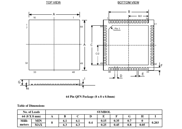
- QFN-64: QFN-64 packages are larger, with dimensions typically ranging from 8mm x 8mm to 10mm x 10mm. They offer a higher pin count, usually up to 64 pins, and may feature multiple rows of pads.
- Comparison Between Different QFN Package Sizes:
- Applications: Smaller QFN package sizes like QFN-16 are suitable for compact electronic devices such as smartphones, wearables, and IoT sensors. Larger sizes like QFN-64 are used in applications requiring higher pin counts and more complex integrated circuits, such as networking equipment and automotive systems.
- Capabilities: Larger QFN package sizes offer greater pin count and signal routing flexibility, making them suitable for high-performance applications with demanding electrical requirements. Smaller packages prioritize space efficiency and are ideal for miniaturized designs with limited board space.
Understanding the dimensions, specifications, and capabilities of common QFN package sizes is essential for selecting the most suitable package for a specific application. By considering factors such as pin count, pad pitch, and overall dimensions, designers can optimize PCB layout, ensure compatibility with assembly processes, and meet the performance requirements of electronic devices across various industries.
Challenges and Solutions in QFN Package Size and Packaging
When designing and manufacturing with QFN Package Size, engineers face several challenges that can impact both the assembly process and the final performance of the device. Understanding these challenges and implementing the right solutions is key to ensuring a reliable and efficient assembly.
Manufacturing Challenges
-
Effects of Package Thickness on Assembly Accuracy
The typical thickness of QFN Package Size ranges from 0.8 mm to 1 mm. This compact size, while advantageous for space-saving, can create difficulties during the assembly process. A thin package may lead to alignment issues during pick-and-place operations, particularly for small QFN Package Sizes like 3×3 mm or 5×5 mm. Misalignment of the component with PCB pads can result in poor solder joints, reducing electrical performance and reliability.
Solution:- Precise pick-and-place equipment: Ensuring the use of high-precision placement machines with accurate vision systems helps align the QFN Package Size perfectly with PCB pads.
- Improved handling: Using specialized fixtures during the assembly process can prevent the QFN Package Size from shifting or tilting, minimizing the risk of misalignment.
-
Common Soldering Issues: Bridging and Voiding
- Bridging: This occurs when solder connects two adjacent pads, causing an unintended short circuit. It is more likely to happen with small QFN Package Sizes due to the tight pitch (e.g., 0.4 mm or 0.5 mm) between the pads.
- Voiding: Voids are gaps in the solder joint that can form due to outgassing during reflow soldering, especially in the thermal pad area. This is a common issue for QFN Package Size designs, where the larger thermal pad may trap gas during the reflow process, leading to voids.
Solution: - Bridging Prevention: To prevent bridging, designers should ensure that the pad size and stencil aperture are correctly sized for the QFN Package Size. Additionally, optimizing the solder paste volume and reflow profile can help mitigate bridging.
- Voiding Reduction: Ensuring proper via design and placement under the thermal pad, as well as controlling the reflow profile, can minimize voiding. Reducing solder paste application in the thermal pad area may also help in preventing void formation. Using solder pastes specifically designed to reduce voiding can further improve the outcome.
Process Improvements
- Optimizing SMT Processes for QFN Assembly
The assembly of QFN Package Size components requires careful optimization of the surface-mount technology (SMT) process to achieve high-quality solder joints and reliable thermal performance. Key improvements in the SMT process include:- Optimizing Stencil Design: Using the right stencil thickness and aperture size for the specific QFN Package Size ensures consistent paste deposition. Smaller packages, like 3×3 mm QFNs, may need a finer stencil to ensure precise paste application.
- Optimized Reflow Profiling: Reflow soldering is the primary method for attaching QFNs to PCBs. An optimized reflow profile is essential to prevent solder defects like bridging, voiding, and insufficient soldering. A slow ramp-up to peak temperature and careful cooling stages can reduce thermal stress and improve solder joint quality.
- Using Fluxing Agents: Applying flux correctly before soldering enhances the wettability of the solder and reduces the risk of poor solder joints. It also helps to improve the adhesion between the QFN pads and the PCB traces.
While QFN Package Size designs present certain challenges in the manufacturing and assembly processes, adopting precision techniques, optimizing SMT processes, and utilizing correct design and soldering practices can mitigate these issues. Ensuring that package thickness, pad designs, and soldering techniques are carefully considered will result in more reliable and efficient QFN packaging.
Get a Quotation ForQFN Package Size Now
Contact Us NOW
FAQs About QFN Package Sizes
What is the standard size of QFN?
The standard size of QFN packages varies, but common sizes range from a few millimeters to around 10mm per side, depending on the pin count and specific requirements of the application.
What are the dimensions of the QFN 16 package?
The QFN-16 package typically has dimensions around 3mm x 3mm, with variations possible depending on the manufacturer and specific design considerations.
What is the height of a QFN package?
The height of a QFN package varies depending on the specific model and manufacturer. However, heights commonly range from around 0.5mm to 1.2mm, again depending on factors such as pin count and application requirements.
What are QFN packages?
QFN (Quad Flat No-leads) packages are a type of surface-mount integrated circuit package characterized by a flat, square or rectangular shape with no external leads extending from the package body. They feature exposed pads on the bottom surface for direct surface mounting onto the PCB, facilitating compact and efficient designs in electronic devices.


发表评论
Want to join the discussion?Feel free to contribute!