
Exploring the Realm of 64-Pin QFN Packages
In the realm of modern electronics, Quad Flat No-leads (QFN) packages have emerged as pivotal components, offering a blend of compactness, efficiency, and performance. These packages revolutionize circuit miniaturization and enhance thermal dissipation, critical in today’s compact electronic devices. Among the myriad QFN variants, the 64-pin QFN package stands out for its versatility and widespread utilization in diverse applications. This specific variant provides an optimal balance between pin count and form factor, making it a preferred choice for various integrated circuits and semiconductor devices. Understanding the intricacies of the 64-pin QFN package unveils insights into its crucial role in advancing electronic engineering.
What is QFN Packaging?
QFN (Quad Flat No-leads) packaging represents a modern innovation in semiconductor packaging, characterized by its compact design and leadless configuration. Unlike traditional packages with protruding leads, QFN packages feature a flat bottom surface with metallic pads for electrical connections, facilitating direct soldering onto the printed circuit board (PCB).
The design and structure of QFN packages incorporate several key elements:
1. Leadless Configuration: QFN packages eliminate the need for external leads, reducing the overall footprint and enabling higher density mounting on PCBs.
2. Exposed Thermal Pad: Many QFN packages include an exposed thermal pad underneath the device, enhancing heat dissipation and improving the thermal performance of the integrated circuit.
3. Variety of Sizes: QFN packages come in various sizes and pin configurations, catering to diverse application requirements ranging from small, low-pin-count devices to larger, high-pin-count ICs.
The versatility of QFN packaging extends across multiple industries, including:
– Consumer Electronics: QFN packages are widely used in smartphones, tablets, laptops, and other portable devices due to their compact size and excellent thermal properties.
– Automotive: QFN packages are employed in automotive applications such as engine control units (ECUs), advanced driver-assistance systems (ADAS), and infotainment systems, where reliability and robustness are paramount.
– Telecommunications: QFN packages find applications in telecommunications equipment, including base stations, routers, and networking devices, benefiting from their high-density integration and reliable performance.
– Industrial and Medical: QFN packages are utilized in industrial automation, medical devices, and instrumentation, where space constraints and reliability are critical factors.
Overall, QFN packaging has become indispensable in modern electronics, offering a balance of size, performance, and reliability across a broad spectrum of industries and applications.
Characteristics of the 64-pin QFN Package
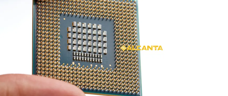
The 64-pin QFN (Quad Flat No-leads) package represents a versatile and widely used variant renowned for its balance of pin count and compact form factor. Here’s a detailed overview of its characteristics:
1. Detailed Description: The 64-pin QFN package features a flat bottom surface with 64 metallic pads arranged around its periphery for electrical connections. These pads facilitate direct surface mounting onto the PCB, eliminating the need for through-hole connections.
2. Dimensions and Layout Specifics: The 64-pin QFN package typically adheres to industry-standard dimensions, with variations in dimensions based on specific manufacturer specifications. Common dimensions include the overall package size (length, width, and height), as well as the pitch between adjacent pads, which determines the spacing between connections.
3. Comparison with Other QFN Package Sizes: In comparison to other QFN package sizes, such as 32-pin or 100-pin variants, the 64-pin QFN strikes a balance between pin count and package size. It offers higher pin density and functionality compared to smaller packages while remaining more compact and cost-effective than larger packages. This makes it suitable for a wide range of applications where space constraints and pin count requirements need to be balanced.
4. Versatility and Applications: The 64-pin QFN package finds applications across various industries, including consumer electronics, telecommunications, automotive, industrial automation, and medical devices. Its versatility makes it suitable for diverse integrated circuits and semiconductor devices, ranging from microcontrollers and sensor ICs to wireless communication modules and power management ICs.
5. Thermal Considerations: Like other QFN packages, the 64-pin variant may feature an exposed thermal pad underneath the device, enhancing its thermal dissipation capabilities. This is particularly beneficial for high-power applications or devices operating in demanding environments where efficient heat management is crucial.
Overall, the 64-pin QFN package offers a compelling combination of compactness, functionality, and thermal performance, making it a popular choice for a wide range of electronic applications requiring moderate pin counts and efficient PCB utilization.
Advantages of QFN Packages
QFN (Quad Flat No-leads) packages offer several advantages over traditional packaging methods, making them a preferred choice in modern electronics. Here’s a detailed exploration of their key advantages:
1. Low Profile and Small Footprint: QFN packages feature a flat bottom surface without protruding leads, resulting in a significantly lower profile compared to packages with leads. This low profile design conserves space on the printed circuit board (PCB), allowing for more compact and sleek electronic devices.
2. Enhanced Thermal and Electrical Performance: The absence of leads in QFN packages reduces parasitic inductance and capacitance, leading to improved electrical performance, including faster signal transmission and reduced signal distortion. Additionally, many QFN packages incorporate an exposed thermal pad underneath the device, enabling efficient heat dissipation and enhancing thermal performance, critical for high-power applications and devices operating in demanding environments.
3. Improved Reliability and Durability: QFN packages are inherently more robust than packages with leads due to their leadless design, which minimizes the risk of lead damage or breakage during handling or thermal cycling. Furthermore, the direct soldering of QFN packages onto the PCB enhances solder joint reliability, reducing the likelihood of solder fatigue or failure over time. This improved reliability translates into greater product durability and longevity, reducing the risk of premature device failure.
4. Suitable for High-Density PCB Designs: QFN packages are ideal for high-density PCB designs where space optimization is crucial. Their compact form factor and low profile enable more efficient use of available PCB real estate, allowing designers to pack more functionality into smaller footprint devices. Additionally, the absence of leads simplifies routing and minimizes signal interference, facilitating high-speed and high-frequency applications.
In summary, QFN packages offer a compelling combination of low profile, enhanced thermal and electrical performance, improved reliability, and suitability for high-density PCB designs. These advantages make them indispensable in a wide range of electronic applications, from consumer electronics and telecommunications to automotive and industrial systems.
Disadvantages of QFN Packages
While QFN (Quad Flat No-leads) packages offer numerous advantages, they also present some disadvantages that warrant consideration in electronic design and manufacturing processes. Here’s a detailed exploration of these drawbacks:
1. Lack of Through-Hole Connections: Unlike some other package types, QFN packages do not feature through-hole connections, which can limit their compatibility with certain PCB designs or assembly methods. Through-hole connections provide additional mechanical support and can be easier to solder manually, making them preferable in some applications where robustness and ease of assembly are paramount.
2. Challenges in Rework and Repair: QFN packages pose challenges in rework and repair processes due to their leadless design and surface-mount nature. Removing and replacing components within a QFN package often requires specialized equipment and techniques, such as hot air rework stations or infrared reflow systems. Additionally, the risk of damaging nearby components or the PCB itself during rework is higher compared to packages with through-hole connections, adding complexity and cost to repair operations.
3. Vulnerability to Solder Joint Cracking Under Stress: The solder joints that connect QFN packages to the PCB are susceptible to mechanical stress, particularly during thermal cycling or mechanical shock events. The absence of leads in QFN packages means that the solder joints bear the full mechanical load, increasing the risk of solder joint cracking or fatigue over time. This vulnerability can compromise the electrical and mechanical integrity of the connection, leading to intermittent or permanent device failure.
Despite these disadvantages, advances in materials, manufacturing techniques, and assembly processes have mitigated many of the challenges associated with QFN packages. Additionally, careful design considerations and adherence to best practices can help minimize the impact of these drawbacks on overall product reliability and performance. As with any packaging technology, weighing the pros and cons of QFN packages is essential to selecting the most suitable option for a given application.
Components of a QFN Package
QFN (Quad Flat No-leads) packages consist of several internal components and structures that contribute to their functionality and performance. Here’s an in-depth overview:
1. Overview of Internal Components: The internal components of a QFN package typically include the integrated circuit (IC) die, connection pads, bonding wires (or copper traces), and optional features such as thermal pads or exposed paddle. The IC die contains the semiconductor device or devices, such as transistors, diodes, or integrated circuits, which perform the intended functions of the package.
2. Connection Pads and Bonding Wires: Connection pads, also known as bond pads, are metallic areas on the surface of the IC die where bonding wires are attached. Bonding wires serve as electrical connections between the die and the external leads or pads of the package. In QFN packages, these connection pads are located around the periphery of the package and are typically made of materials such as gold or aluminum. Alternatively, some QFN packages utilize copper traces instead of bonding wires for direct connection between the IC die and the external pads.
3. Potential Variations in Configurations: QFN packages can exhibit variations in configurations based on factors such as pin count, package size, and specific application requirements. Variations may include differences in pad pitch (the distance between adjacent pads), pad size, pad arrangement (e.g., staggered or aligned), and the presence of additional features such as thermal pads or exposed paddles. Additionally, QFN packages may be available in different materials, such as plastic or ceramic, to accommodate various environmental and performance requirements.
Overall, the internal components of a QFN package are designed to provide reliable electrical connections between the integrated circuit die and the external circuitry, while also optimizing thermal performance and mechanical stability. Understanding these components and their configurations is essential for selecting the most suitable QFN package for a given application.
Applications of 64-pin QFN Packages
The 64-pin QFN (Quad Flat No-leads) package finds extensive use across various industries and devices due to its versatility, compactness, and efficient electrical performance. Here’s a detailed exploration of its applications:
1. Consumer Electronics: The consumer electronics industry extensively utilizes 64-pin QFN packages in devices such as smartphones, tablets, wearables, and digital cameras. These packages are employed for components like microcontrollers, wireless communication modules, power management ICs, and sensor arrays. Their small footprint and high pin count make them ideal for integrating multiple functionalities into compact and sleek consumer devices.
2. Automotive: In the automotive sector, 64-pin QFN packages are deployed in advanced driver-assistance systems (ADAS), engine control units (ECUs), infotainment systems, and vehicle communication networks. Their robust construction, reliability, and thermal performance make them suitable for demanding automotive environments, where resistance to temperature fluctuations, vibration, and moisture is essential.
3. Telecommunications: Telecommunications equipment relies on 64-pin QFN packages for components such as radio frequency (RF) transceivers, baseband processors, and network interface modules. These packages enable high-speed data transmission, efficient power management, and compact designs in networking devices, routers, base stations, and mobile communication systems.
4. Industrial Automation: Industrial automation applications leverage 64-pin QFN packages for controllers, motor drivers, sensors, and monitoring systems. Their small form factor, high pin density, and robust construction support the development of advanced automation solutions for manufacturing, robotics, process control, and industrial IoT (Internet of Things) applications.
5. Medical Devices: In the medical sector, 64-pin QFN packages play a vital role in devices such as patient monitoring systems, medical imaging equipment, diagnostic devices, and implantable medical devices. These packages offer the necessary performance, reliability, and miniaturization required for medical electronics, contributing to advancements in healthcare technology and patient care.
Specific Use Cases Highlighting Advantages:
– A 64-pin QFN package integrated into a handheld medical diagnostic device enables compact design and efficient signal processing, facilitating point-of-care testing and diagnostics in remote or resource-limited settings.
– In an automotive ADAS system, the use of 64-pin QFN packages for sensor fusion and processing units ensures reliable operation and robust performance under harsh environmental conditions, contributing to enhanced vehicle safety and driver assistance features.
– In a wireless communication module for IoT applications, the small footprint and thermal performance of a 64-pin QFN package enable energy-efficient data transmission and seamless integration into IoT devices, supporting connectivity and data exchange in smart home, industrial, and healthcare environments.
Overall, the 64-pin QFN package serves as a foundational technology in a wide range of industries and applications, driving innovation, efficiency, and performance in modern electronic devices and systems.
FAQs about 64 pin qfn package
The number of pins in a QFN (Quad Flat No-leads) package can vary widely depending on the specific design and application requirements. QFN packages can range from a few pins to several hundred pins. However, typical QFN packages often have pin counts ranging from around 8 pins to over 100 pins.
QFN packaging, or Quad Flat No-leads packaging, is a type of surface-mount integrated circuit (IC) package characterized by its flat bottom surface and absence of leads protruding from the sides. Instead of leads, QFN packages feature metallic pads on the bottom surface for electrical connections, allowing for direct soldering onto the printed circuit board (PCB).
QFN packages have some disadvantages, including:
Lack of through-hole connections, which may limit compatibility with certain PCB designs or assembly methods.
Challenges in rework and repair due to the leadless design, requiring specialized equipment and techniques.
Vulnerability to solder joint cracking under stress, particularly during thermal cycling or mechanical shock events.
The components of a QFN package typically include:
Integrated Circuit (IC) Die: Contains the semiconductor device(s) such as transistors, diodes, or integrated circuits.
Connection Pads: Metallic areas on the surface of the IC die where bonding wires or copper traces are attached for electrical connections.
Bonding Wires or Copper Traces: Provide electrical connections between the IC die and the external leads or pads of the package.
Optional Features: Some QFN packages may include additional features such as thermal pads or exposed paddles to enhance thermal dissipation.

