
Efficiency Redefined: 32 QFN Package Advancements
The 32 QFN Package represents a significant advancement in electronic packaging technology. Its compact size and versatility have revolutionized various industries, from consumer electronics to automotive and aerospace. Understanding its intricacies and advantages is crucial for engineers and designers striving for efficiency and performance in their products. By delving into the features and applications of the 32 QFN Package, we can uncover innovative solutions to complex design challenges and enhance the functionality of electronic devices. This exploration aims to shed light on the importance of embracing this packaging form and harnessing its potential for future advancements in technology and product development.
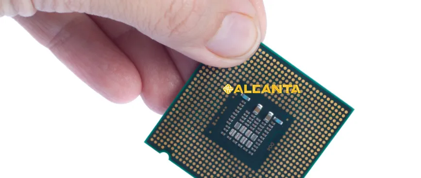
Understanding the 32 QFN Package
The 32 QFN (Quad Flat No-Lead) Package is a type of surface-mount integrated circuit packaging characterized by its compact size, square shape, and absence of leads protruding from the package body. It typically features a square or rectangular footprint with leads on all four sides, facilitating easy soldering to the printed circuit board (PCB).
This packaging variant offers several key characteristics that make it highly desirable in the electronics industry. Firstly, its small form factor allows for high-density PCB designs, making it ideal for applications where space is limited. Additionally, the absence of leads minimizes parasitic inductance and capacitance, resulting in improved electrical performance, reduced signal distortion, and enhanced high-frequency operation.
The 32 QFN Package finds extensive applications across various sectors of the electronics industry. It is commonly employed in mobile devices, such as smartphones and tablets, for housing microcontrollers, RF transceivers, and power management ICs. Furthermore, its compact size and excellent thermal dissipation properties make it suitable for use in automotive electronics, IoT devices, medical equipment, and industrial automation systems.
Overall, the 32 QFN Package’s combination of small footprint, enhanced electrical performance, and versatility makes it a preferred choice for modern electronic designs, enabling manufacturers to develop smaller, more efficient, and high-performance devices to meet the demands of today’s technology-driven world.
Advantages of the 32 QFN Package
The 32 QFN (Quad Flat No-Lead) Package offers several distinct advantages compared to other packaging forms commonly used in the electronics industry.
1. Size and Weight: One of the most significant advantages of the 32 QFN Package is its compact size and lightweight nature. This allows for the development of smaller and lighter electronic devices, making it ideal for applications where space and weight constraints are critical, such as portable consumer electronics and wearable devices.
2. Improved Electrical Performance: The absence of leads in the 32 QFN Package reduces parasitic inductance and capacitance, leading to improved electrical performance. This results in reduced signal distortion, enhanced signal integrity, and better high-frequency operation compared to packages with traditional leaded configurations.
3. Thermal Management: The 32 QFN Package’s design allows for efficient thermal dissipation, enabling better heat transfer from the integrated circuit to the PCB and surrounding environment. This helps in preventing overheating and ensures the reliable operation of electronic components, especially in high-power applications.
4. Cost-Effectiveness: The manufacturing process for 32 QFN Packages involves fewer materials and simpler assembly techniques compared to packages with leads or ball grid arrays (BGAs). This translates to lower production costs, making it a cost-effective solution for mass-produced electronic devices.
5. Mechanical Durability: The 32 QFN Package’s solid construction and lack of exposed leads make it more resistant to mechanical stress and environmental factors such as vibration and shock. This improves the overall reliability and durability of electronic systems, particularly in harsh operating conditions.
The technology and design behind small form-factor packaging like the 32 QFN Package involve advanced manufacturing processes such as semiconductor wafer fabrication, die attachment, wire bonding or flip-chip bonding, encapsulation, and surface-mount assembly. These processes require precision engineering and careful consideration of thermal, electrical, and mechanical factors to ensure optimal performance and reliability. Additionally, advancements in materials science and packaging technologies continue to drive innovation in the design and development of small form-factor packages, further enhancing their advantages and expanding their applications in the electronics industry.
Product Features
The 32 QFN Package boasts a range of product features that set it apart in the realm of integrated circuit packaging. Here’s a detailed overview:
1. Compact Size: One of the most prominent features of the 32 QFN Package is its small footprint. With dimensions typically ranging from a few millimeters to a few centimeters, this compact size allows for high-density integration of components on a PCB, enabling manufacturers to design smaller and more lightweight electronic devices.
2. Enhanced Electrical Performance: The package’s design minimizes parasitic inductance and capacitance, leading to improved electrical performance. This results in reduced signal distortion, enhanced signal integrity, and better overall system reliability, especially in high-frequency applications.
3. Low Power Consumption: The 32 QFN Package is engineered to optimize power efficiency. Its compact size and efficient thermal management contribute to lower power consumption, making it ideal for battery-operated devices and applications where energy efficiency is paramount.
4. Excellent Heat Dissipation: Despite its small size, the 32 QFN Package excels in heat dissipation. The exposed thermal pad on the package’s underside allows for efficient transfer of heat from the integrated circuit to the PCB, preventing overheating and ensuring reliable operation even under demanding conditions.
5. Robust Mechanical Stability: The package’s design includes robust mechanical features, such as corner and side castellations, ensuring secure attachment to the PCB during assembly processes like soldering and reflow. This enhances the overall durability and reliability of the electronic device.
6. Versatility: The 32 QFN Package is versatile and can accommodate a wide range of semiconductor devices, including microcontrollers, RF transceivers, power management ICs, and sensors. Its compatibility with various applications makes it a preferred choice across different industries.
In summary, the 32 QFN Package offers a compelling array of features, including compact size, enhanced electrical performance, low power consumption, excellent heat dissipation, robust mechanical stability, and versatility. These features collectively contribute to the package’s superiority in performance, reliability, and efficiency, making it an indispensable component in modern electronic designs.
Application Scenarios
The versatility and compact design of the 32 QFN Package make it suitable for a wide range of application scenarios across diverse industries. Here’s a detailed exploration:
1. Consumer Electronics: In smartphones, tablets, wearables, and other portable devices, the 32 QFN Package finds extensive use for microcontrollers, wireless communication modules, and power management ICs. Its small footprint allows for sleek and compact device designs while maintaining high performance and efficiency.
2. Automotive Electronics: Automotive electronics benefit from the 32 QFN Package’s compact size and excellent thermal management. It is commonly employed in advanced driver assistance systems (ADAS), infotainment systems, engine control units (ECUs), and sensor modules, where space is limited, and reliability is paramount.
3. Industrial Automation: In industrial automation applications, such as PLCs (Programmable Logic Controllers), motor control systems, and sensor networks, the 32 QFN Package offers high reliability and performance in harsh operating environments. Its small form factor enables space-saving designs in control cabinets and machinery.
4. Internet of Things (IoT): IoT devices often require compact and energy-efficient components, making the 32 QFN Package an ideal choice for sensor nodes, communication modules, and edge computing devices. Its low power consumption and robust design make it well-suited for continuous operation in IoT networks.
5. Medical Devices: Medical electronics demand high reliability and precision, making the 32 QFN Package a preferred option for applications such as wearable health monitors, diagnostic equipment, and implantable devices. Its small size allows for non-intrusive integration into medical devices while ensuring reliable performance.
Real-world examples of the 32 QFN Package’s application include:
– Using it in a smart thermostat for home automation systems, where its small size and low power consumption are crucial for seamless integration and long battery life.
– Implementing it in an automotive radar sensor for collision avoidance systems, leveraging its compact design and robust thermal management for reliable operation in extreme temperature conditions.
– Integrating it into a wireless sensor node for industrial monitoring applications, where its small form factor and high reliability ensure accurate data collection and transmission in harsh industrial environments.
Overall, the 32 QFN Package’s adaptability, reliability, and performance make it an integral component in a diverse array of application scenarios, driving innovation and advancement across industries.
Design and Layout Recommendations
When designing and laying out a PCB (Printed Circuit Board) with the 32 QFN Package, several key considerations can enhance both performance and reliability:
1. Thermal Management: Ensure proper thermal management by incorporating a thermal pad on the PCB layout, directly under the package. This allows efficient dissipation of heat generated by the integrated circuit, preventing overheating and ensuring long-term reliability. Additionally, consider adding thermal vias to conduct heat away from the package to inner layers of the PCB.
2. Placement and Routing: Strategically place the 32 QFN Package on the PCB to minimize signal interference and optimize signal integrity. Place sensitive analog or high-speed digital traces away from noisy components and high-current paths. Implement controlled impedance traces for high-frequency signals to minimize signal loss and reflections.
3. Power Integrity: Pay close attention to power distribution and decoupling capacitor placement to ensure stable power delivery to the 32 QFN Package and other components on the PCB. Use multiple vias to connect the power and ground planes to reduce impedance and minimize voltage drops, especially in high-current paths.
4. Signal Integrity: Maintain signal integrity by keeping signal traces short and direct, minimizing trace lengths and avoiding sharp bends or right angles. Use differential pairs for high-speed data signals to improve noise immunity and reduce electromagnetic interference (EMI). Implement proper termination techniques, such as series termination resistors, to mitigate signal reflections and ensure clean signal transitions.
5. Manufacturability and Assembly: Design the PCB layout with manufacturability and assembly in mind. Ensure adequate spacing between components and traces to accommodate soldering and assembly processes. Follow industry-standard design guidelines for solder mask, solder stencil, and assembly drawings to facilitate smooth manufacturing processes and ensure consistent quality.
6. Reliability Testing: Conduct thorough reliability testing, including thermal cycling, vibration testing, and accelerated aging tests, to validate the performance and robustness of the PCB design with the 32 QFN Package. Identify and address any potential reliability issues during the design phase to prevent costly failures in the field.
Emphasizing the importance of good design practices throughout the design and layout process is critical for achieving optimal performance and reliability with the 32 QFN Package. By following these recommendations and leveraging advanced PCB design tools and simulation techniques, engineers can develop high-quality, reliable electronic systems that meet the demands of today’s technology-driven applications.
Production and Manufacturing of the 32 QFN Package
The production and manufacturing process of the 32 QFN Package involves several key steps to ensure high-quality and reliable end products.
1. Design and Prototyping: The process begins with the design of the 32 QFN Package, where engineers use specialized CAD software to create the package layout and design features. Prototyping follows, allowing for testing and validation of the design before mass production.
2. Wafer Fabrication: The heart of the manufacturing process lies in wafer fabrication. This involves the creation of semiconductor wafers through processes like photolithography, etching, deposition, and doping. Each wafer contains numerous individual 32 QFN Package units.
3. Die Bonding: After wafer fabrication, individual dies (integrated circuits) are separated and bonded onto the lead frames of the 32 QFN Package. Precision die bonding equipment is used to ensure accurate placement and alignment of the dies onto the package substrate.
4. Wire Bonding: Once the dies are bonded, wire bonding is performed to connect the die to the package leads using thin wires made of gold or aluminum. Wire bonding machines precisely bond each wire to its designated pad on the die and the lead frame, forming electrical connections.
5. Molding: The wire-bonded assembly is encapsulated in a protective material through molding. This protects the delicate wires and die from environmental factors such as moisture, dust, and mechanical stress. Molding compounds are chosen for their thermal conductivity, adhesion properties, and resistance to chemical and mechanical stresses.
6. Singulation: After molding, the individual 32 QFN Packages are singulated from the lead frame using precision sawing equipment. This separates the packages while maintaining tight tolerances to ensure uniformity and consistency.
7. Testing and Quality Control: Each 32 QFN Package undergoes rigorous testing to ensure adherence to quality standards and specifications. This includes electrical testing to verify functionality, performance, and reliability. Additionally, visual inspection and automated optical inspection (AOI) are conducted to detect any defects or anomalies in the package.
8. Packaging and Shipping: Once testing and quality control are completed, the 32 QFN Packages are packaged and labeled according to customer requirements. They are then shipped to electronics manufacturers for integration into various end products.
Quality Control and Manufacturing Standards
Quality control is paramount in the production and manufacturing of the 32 QFN Package to ensure consistent performance and reliability. Manufacturers adhere to industry standards such as ISO 9001 for quality management systems and ISO 14001 for environmental management systems. Additionally, they may follow specific industry standards such as IPC-A-610 for electronic assembly and J-STD-020 for moisture sensitivity.
Strict quality control measures are implemented at each stage of the manufacturing process, including incoming materials inspection, process monitoring, and final product testing. This ensures that only high-quality and defect-free 32 QFN Packages are delivered to customers.
By adhering to stringent quality control and manufacturing standards, manufacturers can guarantee the reliability and performance of the 32 QFN Package, meeting the demanding requirements of various industries and applications.
Future Development Trends of the 32 QFN Package
As technology continues to advance, the 32 QFN Package is expected to evolve to meet the evolving needs of the electronics industry. Here’s an outlook on future development trends and potential innovations:
1. Miniaturization: The trend towards smaller and more compact electronic devices is likely to continue, driving the demand for even smaller 32 QFN Packages. Manufacturers will focus on further miniaturizing the package while maintaining or enhancing its electrical performance and reliability.
2. Higher Integration: There will be a growing demand for higher levels of integration within electronic devices, requiring 32 QFN Packages to accommodate more complex and feature-rich semiconductor components. This trend will drive innovations in package design, substrate materials, and interconnect technologies to support increased functionality within smaller footprints.
3. Enhanced Thermal Management: With the increasing power densities of semiconductor devices, thermal management will remain a critical consideration for the 32 QFN Package. Future developments may include advanced thermal interface materials, innovative package designs, and enhanced heat dissipation techniques to address the challenges of thermal management in high-performance applications.
4. Advanced Materials: The use of advanced materials, such as new substrate materials and lead frame alloys, may offer opportunities for improving the performance, reliability, and manufacturability of the 32 QFN Package. Innovations in material science will enable the development of packages with superior electrical, thermal, and mechanical properties.
5. 3D Integration: Three-dimensional (3D) integration technologies, such as chip stacking and through-silicon vias (TSVs), hold promise for enhancing the functionality and performance of the 32 QFN Package. Future developments may focus on integrating multiple dies within a single package, enabling higher levels of integration and improved system performance.
6. Advanced Packaging Technologies: Emerging packaging technologies, such as fan-out wafer-level packaging (FOWLP) and system-in-package (SiP) integration, offer opportunities for enhancing the capabilities of the 32 QFN Package. These technologies enable heterogeneous integration of diverse components, including multiple dies, passive components, and MEMS devices, within a single package, providing increased functionality and performance.
7. IoT and Edge Computing: The proliferation of IoT devices and edge computing applications will drive demand for 32 QFN Packages with optimized power consumption, enhanced connectivity, and increased processing capabilities. Future developments may focus on integrating specialized features, such as on-chip security, sensor interfaces, and low-power wireless communication protocols, to support the requirements of IoT and edge computing applications.
In summary, the future development trends of the 32 QFN Package will be driven by the need for smaller size, higher integration, improved thermal management, advanced materials, 3D integration, advanced packaging technologies, and the requirements of emerging applications such as IoT and edge computing. By embracing these trends and driving innovation, manufacturers can continue to push the boundaries of performance, functionality, and reliability in the 32 QFN Package, enabling the development of next-generation electronic devices and systems.
FAQs about 32 qfn package
The 32 QFN package is a type of surface-mount integrated circuit packaging characterized by its compact size, square shape, and absence of leads protruding from the package body. It typically features a square or rectangular footprint with leads on all four sides.
The 32 QFN package offers several advantages, including a small form factor for high-density PCB designs, enhanced electrical performance with minimized parasitic inductance and capacitance, low power consumption, and excellent heat dissipation properties.
The 32 QFN package finds extensive applications across various industries, including consumer electronics (e.g., smartphones, tablets), automotive electronics (e.g., ADAS, infotainment systems), industrial automation, IoT devices, and medical electronics.
Design considerations for the 32 QFN package include thermal management to ensure efficient heat dissipation, proper placement and routing of traces to optimize signal integrity, power integrity to ensure stable power delivery, and manufacturability and assembly to facilitate smooth production processes.

