
The Backbone of Electronics: Packaging Substrate Manufacturers
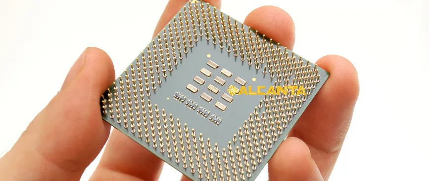
Packaging substrate manufacturers play a pivotal role in the production of essential components for electronic devices. These manufacturers specialize in crafting substrates, which serve as the foundational layer for integrated circuits (ICs) and other electronic components. Essentially, packaging substrates provide the structural support and electrical pathways necessary for the functioning of semiconductor devices.
The significance of packaging substrates lies in their ability to ensure the reliability, performance, and longevity of electronic products. As technology advances and devices become increasingly complex and compact, the demand for high-quality packaging substrates continues to rise. In this overview, we’ll delve into the realm of packaging substrate manufacturers, examining their contributions to the electronics industry and the intricate processes involved in substrate manufacturing.
Understanding Substrates in Packaging
In the realm of electronics packaging, substrates serve as the fundamental building blocks upon which integrated circuits (ICs) and electronic components are constructed. These substrates provide the necessary structural support and electrical connections for the components they encapsulate. Understanding the different types of substrates used in packaging is crucial for comprehending their diverse applications and functionalities.
Types of Substrates Used in Packaging
1. Organic Substrates: Organic substrates, commonly referred to as printed circuit boards (PCBs), are composed of organic materials such as epoxy resin and fiberglass. These substrates are lightweight, cost-effective, and offer excellent electrical insulation properties. They are widely used in consumer electronics, automotive applications, and telecommunications equipment.
2. Inorganic Substrates: Inorganic substrates are typically made of ceramics such as alumina (Al2O3) or aluminum nitride (AlN). These substrates exhibit superior thermal conductivity, mechanical strength, and stability at high temperatures, making them ideal for applications requiring robust performance, such as power modules and high-power LED lighting.
3. Hybrid Substrates: Hybrid substrates combine organic and inorganic materials to leverage the advantages of both types. For instance, a common hybrid substrate consists of a ceramic core with organic layers on top for circuit routing. These substrates offer a balance between performance, cost, and manufacturability, catering to a wide range of electronic applications.
Role of Substrates in Packaging: Packaging substrates play a crucial role in the overall performance, reliability, and functionality of electronic devices. Their primary functions include:
- Providing mechanical support and protection for delicate semiconductor components.
- Facilitating electrical connections between integrated circuits, passive components, and external interfaces.
- Dissipating heat generated during device operation to prevent overheating and ensure optimal performance.
- Enabling miniaturization and densification of electronic assemblies by providing compact, high-density interconnect solutions.
In essence, packaging substrates serve as the backbone of electronic packaging, enabling the seamless integration of semiconductor devices into various electronic products. Understanding the different types and roles of substrates is essential for selecting the most suitable materials and designs to meet the specific requirements of each application.
Understanding Substrates in Packaging: Exploring the Role and Types Offered by Packaging Substrate Manufacturers
Types of Substrates Used in Packaging
1. Organic Substrates: Packaging substrate manufacturers commonly produce organic substrates, also known as printed circuit boards (PCBs). These substrates are crafted from materials like epoxy resin and fiberglass. Organic substrates are favored for their lightweight nature, cost-effectiveness, and excellent electrical insulation properties. They find extensive use in various electronic applications, including consumer electronics, automotive systems, and telecommunications equipment.
2. Inorganic Substrates: Inorganic substrates, often composed of ceramics such as alumina (Al2O3) or aluminum nitride (AlN), are another specialty of packaging substrate manufacturers. These substrates boast superior thermal conductivity, mechanical strength, and stability at high temperatures. Consequently, they are preferred for demanding applications such as power modules and high-power LED lighting, where robust performance is paramount.
3. Hybrid Substrates: Hybrid substrates, a synthesis of organic and inorganic materials, are engineered to harness the strengths of both categories. One prevalent hybrid substrate configuration involves a ceramic core with organic layers for circuit routing. These substrates strike a balance between performance, cost, and manufacturability, catering to diverse electronic applications across industries.
Role of Substrates in Packaging: Packaging substrate manufacturers play a pivotal role in the electronics industry by providing substrates that serve critical functions in electronic packaging:
- Mechanical Support and Protection: Substrates offer structural integrity and safeguard delicate semiconductor components from mechanical stress and environmental factors.
- Electrical Connectivity: Substrates facilitate electrical connections between integrated circuits, passive components, and external interfaces, ensuring seamless functionality.
- Heat Dissipation: Efficient heat dissipation is vital for maintaining device reliability and performance. Substrates help dissipate heat generated during operation, thereby preventing thermal issues.
- Miniaturization and Densification: With advancements in technology, substrates enable the miniaturization and densification of electronic assemblies, contributing to the development of compact and high-performance devices.
Understanding the diverse types and roles of substrates provided by packaging substrate manufacturers is essential for selecting suitable materials and designs to meet the specific requirements of various electronic applications.
Key Players in Packaging Substrate Manufacturing
AT&S
Company Overview: AT&S (Austria Technologie & Systemtechnik Aktiengesellschaft) is a prominent player in the field of packaging substrate manufacturing. Founded in 1987 and headquartered in Leoben, Austria, AT&S has established itself as a leading provider of high-quality substrates for various electronic applications worldwide.
Products and Services: AT&S offers a diverse range of advanced packaging substrates tailored to meet the evolving needs of the electronics industry. Their product portfolio includes:
- High-density interconnect (HDI) substrates
- IC substrates
- Substrates for automotive electronics
- Substrates for mobile devices and telecommunications
- Advanced packaging solutions for emerging technologies like 5G and IoT devices
AT&S also provides comprehensive design, manufacturing, and testing services to ensure the reliability and performance of their substrates across diverse applications.
Market Position: AT&S holds a strong position in the global packaging substrate market, thanks to its commitment to innovation, quality, and customer satisfaction. With a robust presence in key markets such as Europe, Asia, and North America, AT&S continues to expand its market share and strengthen its position as a trusted supplier of advanced packaging solutions.
Ibiden
Company Overview: Ibiden Co., Ltd. is a renowned Japanese company specializing in the development and manufacture of advanced packaging substrates. Established in 1912 and headquartered in Ogaki, Japan, Ibiden has a rich history of innovation and technological expertise in the electronics industry.
Products and Services: Ibiden offers a comprehensive range of packaging substrates designed to meet the stringent requirements of modern electronic devices. Their product offerings include:
- High-density interconnect (HDI) substrates
- IC substrates for semiconductor packaging
- Substrates for automotive electronics and power modules
- Substrates for smartphones, tablets, and other mobile devices
- Environmentally-friendly substrates with a focus on sustainability
In addition to substrate manufacturing, Ibiden provides value-added services such as design support, thermal management solutions, and quality assurance to ensure the success of their customers’ projects.
Market Position: Ibiden maintains a prominent position in the global packaging substrate market, driven by its strong reputation for quality, reliability, and technological innovation. With a presence in key markets across Asia, Europe, and North America, Ibiden continues to expand its market share and solidify its position as a leading supplier of advanced packaging solutions.
Unimicron
Company Overview: Unimicron Technology Corporation is a Taiwanese company specializing in the design and manufacture of high-performance packaging substrates. Founded in 1990 and headquartered in Taoyuan City, Taiwan, Unimicron has emerged as a key player in the global electronics industry.
Products and Services: Unimicron offers a wide range of packaging substrates tailored to meet the diverse needs of its customers. Their product portfolio includes:
- High-density interconnect (HDI) substrates
- IC substrates for semiconductor packaging
- Substrates for automotive electronics and industrial applications
- Substrates for communication equipment and networking devices
- Advanced materials and technologies for next-generation electronic products
Unimicron also provides comprehensive services such as substrate design, testing, and quality assurance to ensure the performance and reliability of their products.
Market Position: Unimicron holds a significant position in the global packaging substrate market, driven by its focus on innovation, quality, and customer satisfaction. With manufacturing facilities and sales offices strategically located across Asia, Europe, and North America, Unimicron continues to strengthen its presence in key markets and expand its market share in the electronics industry.
Substrate Manufacturing Process: Insights into Packaging Substrate Manufacturers
Overview of Substrate Manufacturing: Packaging substrate manufacturing involves a complex series of processes aimed at fabricating substrates that meet the stringent requirements of modern electronic devices. Packaging substrate manufacturers employ state-of-the-art equipment and advanced techniques to produce substrates with high precision, reliability, and performance.
Key Steps in the Manufacturing Process: The packaging substrate fabrication process typically includes the following key steps:
- Material Selection: Packaging substrate manufacturers carefully select materials based on the specific requirements of the application, considering factors such as electrical conductivity, thermal performance, mechanical strength, and cost-effectiveness.
- Substrate Formation: The selected materials are processed to form the substrate base, which may involve techniques such as lamination, pressing, or casting. This step ensures the substrate’s structural integrity and dimensional accuracy.
- Circuit Patterning: Substrates are then subjected to circuit patterning processes, where conductive traces, vias, and pads are etched onto the substrate surface using photolithography, chemical etching, or laser ablation techniques. This step establishes the electrical pathways necessary for interconnecting electronic components.
- Surface Treatment: Surface treatment processes such as metallization, solder mask application, and surface finish deposition are performed to enhance the substrate’s electrical performance, solderability, and corrosion resistance.
- Quality Control: Throughout the manufacturing process, rigorous quality control measures are implemented to ensure the substrates meet the specified tolerances, performance criteria, and reliability standards. This may involve various inspection techniques such as optical inspection, electrical testing, and mechanical testing.
- Packaging and Shipping: Once the substrates pass quality control checks, they are packaged and prepared for shipment to customers, where they will be integrated into electronic assemblies or devices.
Technologies and Innovations: Packaging substrate manufacturers continually invest in research and development to drive technological advancements and innovation in substrate manufacturing. Some notable technologies and innovations include:
- Advanced materials and composites to enhance substrate performance and reliability.
- High-precision manufacturing equipment and processes for tighter tolerances and finer features.
- Novel circuit patterning techniques such as additive manufacturing and direct-write lithography.
- Integration of embedded components and passive devices within the substrate structure to improve space utilization and functionality.
- Implementation of Industry 4.0 principles, such as automation, data analytics, and digitalization, to streamline manufacturing processes and enhance productivity.
By embracing these technologies and innovations, packaging substrate manufacturers can stay competitive in the dynamic electronics industry, offering cutting-edge substrates that meet the evolving demands of electronic applications.
Applications of Packaging Substrates: Exploring Diverse Industries Served by Packaging Substrate Manufacturers
Consumer Electronics
Packaging substrate manufacturers play a crucial role in the consumer electronics industry by supplying substrates for a wide range of devices, including smartphones, tablets, laptops, and wearables. These substrates enable the miniaturization and integration of electronic components, contributing to the sleek and compact designs of modern gadgets. Advanced packaging substrate fabrication techniques ensure high-density interconnects, improved thermal management, and enhanced reliability, meeting the stringent requirements of consumer electronics manufacturers.
Automotive Industry
In the automotive industry, packaging substrates are essential components used in various electronic systems, including engine control units, infotainment systems, advanced driver-assistance systems (ADAS), and electric vehicle (EV) powertrains. Packaging substrate manufacturers provide substrates with superior thermal performance, high reliability, and automotive-grade durability to withstand harsh operating conditions. These substrates enable the implementation of advanced electronic features, enhancing vehicle safety, efficiency, and connectivity.
Aerospace and Defense
Packaging substrates play a critical role in aerospace and defense applications, where reliability, performance, and ruggedness are paramount. Manufacturers supply substrates for avionics systems, radar systems, communication equipment, and missile guidance systems. Advanced packaging substrate fabrication techniques ensure compliance with stringent military standards and specifications, including high-temperature operation, vibration resistance, and radiation tolerance, enabling the deployment of mission-critical electronic systems in aerospace and defense platforms.
Medical Devices
In the medical device industry, packaging substrates are utilized in a wide range of applications, including diagnostic equipment, patient monitoring systems, implantable devices, and medical imaging devices. Packaging substrate manufacturers supply substrates with biocompatible materials, excellent electrical properties, and high reliability to meet the stringent requirements of medical device manufacturers. These substrates enable the development of innovative medical technologies that enhance patient care, diagnosis, and treatment outcomes.
Others
Packaging substrate manufacturers cater to diverse industries beyond consumer electronics, automotive, aerospace, and medical devices. Their substrates find applications in industrial automation, telecommunications infrastructure, energy systems, and IoT (Internet of Things) devices. By providing customized substrates with advanced features such as high-speed signaling, signal integrity, and power distribution, manufacturers support the development of cutting-edge technologies across various sectors, driving innovation and progress in the global marketplace.
Advancements and Trends in Packaging Substrates: Driving Innovation in the Industry by Packaging Substrate Manufacturers
Miniaturization and High-Density Interconnects
Packaging substrate manufacturers are at the forefront of enabling miniaturization and high-density interconnects in electronic devices. With the demand for smaller, lighter, and more powerful gadgets increasing, suppliers are developing advanced fabrication techniques to produce substrates with tighter pitch, finer traces, and increased layer counts. These substrates facilitate the integration of complex electronic components in compact form factors, allowing manufacturers to create innovative products with enhanced functionality and performance.
Advanced Materials and Technologies
Packaging substrate manufacturers are constantly exploring new materials and technologies to improve the performance and reliability of their products. Advancements in materials science, such as the development of low-loss dielectrics, high thermal conductivity substrates, and novel bonding techniques, enable the creation of substrates with superior electrical, thermal, and mechanical properties. Additionally, the adoption of advanced manufacturing processes, such as laser drilling, additive manufacturing, and 3D printing, allows packaging substrate suppliers to achieve greater precision, flexibility, and efficiency in substrate fabrication.
Environmental Sustainability
In response to growing concerns about environmental sustainability, packaging substrate manufacturers are increasingly focusing on eco-friendly practices and materials. Suppliers are investing in research and development to reduce the environmental impact of their operations and products. This includes the use of recycled materials, eco-friendly manufacturing processes, and the development of biodegradable substrates. By embracing sustainable practices, packaging substrate suppliers not only contribute to environmental conservation but also meet the sustainability requirements of their customers and regulatory bodies, ensuring a greener future for the electronics industry.
Future Outlook and Challenges: Navigating the Path Ahead for Packaging Substrate Manufacturers
Market Projections
The future looks promising for packaging substrate manufacturers as the demand for advanced electronic devices continues to rise across various industries. Market projections indicate sustained growth driven by trends such as the proliferation of IoT devices, the adoption of 5G technology, and the increasing integration of electronics in automotive and medical applications. As a result, packaging substrate suppliers are expected to experience heightened demand for their products and services, fueling expansion and innovation in the industry.
Regulatory Environment
Packaging substrate manufacturers face evolving regulatory requirements aimed at ensuring product safety, environmental sustainability, and compliance with industry standards. Regulatory initiatives such as RoHS (Restriction of Hazardous Substances) directives and REACH (Registration, Evaluation, Authorization, and Restriction of Chemicals) regulations pose challenges for packaging substrate suppliers in terms of material selection, waste management, and product labeling. Navigating the complex regulatory landscape requires continuous monitoring, adaptation, and investment in compliance measures to maintain market access and reputation.
Technological Challenges and Opportunities
While technological advancements present opportunities for packaging substrate manufacturers, they also bring about challenges that must be addressed to stay competitive in the market. Technological challenges include meeting the demand for higher density interconnects, addressing thermal management issues in compact devices, and ensuring signal integrity in high-speed applications. Additionally, the emergence of new materials, manufacturing processes, and design requirements necessitates ongoing investment in research and development to stay at the forefront of innovation. By embracing technological advancements and overcoming challenges, packaging substrate suppliers can seize opportunities for growth and differentiation in the dynamic electronics industry landscape.
As packaging substrate manufacturers navigate the future, they must stay vigilant, adaptable, and innovative to capitalize on market opportunities, navigate regulatory complexities, and address technological challenges effectively. By doing so, they can continue to drive progress and shape the future of the electronics industry.
FAQs About Packaging Substrate Manufacturers
Substrates used in packaging vary depending on the application but commonly include organic substrates (such as printed circuit boards or PCBs), inorganic substrates (like ceramic substrates), and hybrid substrates (a combination of organic and inorganic materials).
Substrate manufacturing involves the process of producing the foundational layers on which integrated circuits and electronic components are built. It includes various steps such as material selection, fabrication, patterning, and quality assurance to create substrates with desired properties and functionality.
In IC packaging, a substrate refers to the base material onto which semiconductor chips are mounted and interconnected. It provides mechanical support, electrical connections, and thermal management for the semiconductor device, ensuring its proper functioning within the electronic system.
A semiconductor package substrate is a specialized substrate used in semiconductor packaging to house and interconnect semiconductor chips or dies. These substrates are designed to meet specific electrical, thermal, and mechanical requirements of semiconductor devices, ensuring reliable performance and integration within electronic systems.


发表评论
Want to join the discussion?Feel free to contribute!