
Key Considerations for Effective Flexible PCB Design
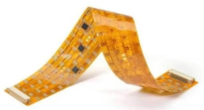
Flexible PCB design refers to the process of creating printed circuit boards that can bend, twist, or fold without damaging the circuitry. Unlike traditional rigid PCBs, which are made from stiff materials and cannot be flexed, flexible PCBs are built using materials like polyimide, allowing for dynamic or static flexibility. The main difference lies in their construction and application—rigid PCBs are ideal for flat, stable surfaces, while flexible PCBs are perfect for compact or irregularly shaped electronic products. Flexible PCB design is commonly used in wearables, medical devices, aerospace systems, and other space-constrained electronics due to its lightweight and space-saving properties. It’s also important to understand the difference between PCB (Printed Circuit Board) and PWB (Printed Wiring Board). While often used interchangeably, PWB typically refers to boards without mounted components, whereas PCB implies a populated board.
Reference: Wevolver
Core Materials Used in Flexible PCB Design
A crucial part of successful flexible pcb design is understanding the materials that form the foundation of a reliable and bendable circuit. Each layer and component impacts the board’s flexibility, performance, and cost.
Polyimide (PI) is the most common base material used in flexible pcb design due to its excellent thermal stability, chemical resistance, and mechanical flexibility. It allows the board to bend repeatedly without cracking or delaminating, making it ideal for dynamic applications.
PET (Polyester) is another option, more affordable than PI, but with lower heat resistance. It’s typically used in low-cost, static-flex applications.
Adhesives (like acrylic or epoxy) are used to bond copper to the substrate and between layers. The choice of adhesive affects overall thickness, flexibility, and thermal reliability.
Copper foil serves as the conductive layer. Rolled annealed (RA) copper is preferred in flexible pcb design for its superior ductility over electrodeposited (ED) copper.
Reference: PCBCart Material Guide
Key Design Guidelines for Flexible PCB Design
A successful flexible pcb design follows a well-structured approach that balances mechanical flexibility with electrical performance. The general design flow begins with defining mechanical constraints, selecting materials, planning stack-ups, and verifying bend behavior before moving into layout and final fabrication checks.
Several critical parameters must be considered during flexible pcb design:
-
Bend radius: Maintaining a proper bend radius is vital to avoid cracking. A typical rule is that the bend radius should be at least 10 times the board thickness for dynamic applications.
-
Trace width and spacing: Wider traces with rounded corners reduce stress. Keep traces parallel to the bend direction and avoid sharp angles.
-
Impedance control: For high-speed signals, impedance must be tightly managed, which can be challenging in a flexible environment due to varying dielectric properties.
-
Layer stack-up: In flexible pcb design, single- or double-sided stacks are common, while rigid-flex designs require complex hybrid layering to manage both flexibility and rigidity.
-
Transition zones: The interface between rigid and flexible regions should avoid copper overlap or sharp edges, as stress tends to concentrate here.
-
DFM considerations: Collaborate early with manufacturers to ensure the design can be fabricated without issues such as delamination, etching defects, or layer misalignment.
For more detailed recommendations, the ProtoExpress design guidelines and the Hemeixin Design Guide offer valuable insights specific to real-world flexible pcb design applications.
Software Tools for Flexible PCB Design
Choosing the right EDA software is essential for efficient and accurate flexible pcb design. Not all design tools offer the same level of support for flex and rigid-flex layouts, so it’s important to select one that aligns with your project’s complexity and requirements.
Altium Designer is widely regarded as one of the most advanced tools for flexible pcb design. It features dynamic bend modeling, allowing engineers to simulate how the board will behave when flexed. The software also includes powerful 3D stack visualization, which is especially useful in rigid-flex designs where spatial constraints are tight.
KiCad, a popular open-source alternative, does offer basic support for flexible pcb design, including curved traces and shape-based board outlines. However, it lacks native support for dynamic bending simulation and stack-up management, making it better suited for simpler designs.
Other tools like Eagle and OrCAD provide some flex PCB layout capabilities, but may require manual workarounds or third-party integrations for complex stack-up visualization and mechanical simulations.
Community discussions offer valuable real-world insight. A Reddit thread highlights user experiences and helpful learning resources for flexible pcb design, while the KiCad Forum provides specific guidance for implementing flex layouts in KiCad.
Common Challenges and Solutions in Flexible PCB Design
Although flexible pcb design offers numerous advantages in compact and dynamic applications, it also presents unique engineering challenges that must be addressed to ensure performance and reliability.
Managing mechanical stress in flex zones is one of the most critical aspects of flexible pcb design. Repeated bending can lead to copper fatigue, trace cracking, or delamination. Solutions include using rolled annealed copper for better ductility, routing traces perpendicular to bend axes, and maintaining appropriate bend radii to minimize stress concentration.
Reliable stack-up construction is also essential. In flexible pcb design, the layer configuration must balance flexibility with electrical performance. Improper bonding or uneven thickness can lead to warping or mechanical failure, especially in rigid-flex designs.
Connector and component placement strategy is vital. Avoid placing components in active bend areas, and use strain relief features like fillets or teardrops near vias and pads to reduce mechanical stress.
EMI/EMC design challenges are often intensified in flexible circuit design due to thinner dielectric materials and the board’s ability to move. Shielding, ground planes, and controlled impedance traces are key solutions for mitigating signal interference.
Lifecycle and durability testing is crucial to verify design reliability. Flex boards should undergo dynamic bend testing, thermal cycling, and vibration testing based on the application environment.
So, are flexible PCBs reliable? When designed and tested properly, the answer is yes—they can deliver long-lasting, high-performance solutions even in harsh conditions.
Rigid-Flex PCB Design Tips in Flexible PCB Design
A hybrid approach to flexible pcb design involves integrating both rigid and flexible sections into a single board—commonly known as rigid-flex PCBs. These are especially useful in devices requiring high reliability in tight or foldable configurations, such as cameras, medical instruments, and aerospace controls.
A key element of flexible pcb design in rigid-flex structures is managing the transition from rigid to flex zones. Sharp corners, copper layers ending abruptly, or inconsistent stack-up at the junctions can lead to delamination or cracking. Designers should use gradual tapering, controlled trace routing, and reinforced materials to handle these transitions smoothly.
Stack-up considerations for hybrid boards are more complex than in pure rigid or flexible designs. In these boards, rigid sections require strong mechanical layers, while flexible regions need lightweight, bendable substrates. Proper lamination sequencing and adhesive selection ensure both flexibility and strength in the final assembly.
Understanding the difference between dynamic vs static bending design approaches is also essential. Static bend designs are folded during assembly and never flex again, while dynamic applications undergo repeated movement. Each use case demands specific materials, copper types, and trace routing rules to ensure longevity.
For comprehensive design practices, the ProtoExpress Rigid-Flex Guide offers valuable tips tailored for rigid-flex implementations within a flexible pcb design workflow.
Advantages and Disadvantages of Flexible PCBs in Flexible PCB Design
Understanding the benefits and limitations is crucial when evaluating whether flexible pcb design is the right choice for your project. While this technology offers compelling advantages, it also introduces specific challenges that must be considered early in the design process.
Pros of Flexible PCB Design
-
Space and weight savings: One of the biggest advantages of flexible pcb design is its ability to significantly reduce both size and weight. By eliminating the need for bulky connectors and routing paths, designers can optimize every millimeter of space in compact devices.
-
Greater design freedom and mechanical flexibility: Flexible PCBs allow boards to bend, twist, or fold to fit into unconventional shapes. This enables innovation in wearable tech, medical implants, and aerospace systems, where rigid boards would simply not fit.
Cons of Flexible PCB Design
-
Higher cost and complexity: Compared to traditional boards, flexible circuit design typically involves more expensive materials, longer prototyping cycles, and tighter design tolerances. This can drive up the overall project cost—especially for low-volume production.
-
Requires precise manufacturing: Requires precise manufacturing: Fabrication of flexible circuits demands specialized equipment and expertise. Even slight errors in alignment, lamination, or adhesive application can lead to failure. Partnering with an experienced manufacturer is essential to successful circuit design.
For a more detailed comparison of pros and cons, refer to the guide by Proto-Electronics.
Manufacturing Considerations in Flexible PCB Design
Successful flexible pcb design doesn’t end at layout—it must translate effectively into manufacturable output. Because of the specialized materials and processes involved, working closely with experienced fabricators is essential to ensure quality and yield.
Partnering with manufacturers that specialize in flexible pcb design, such as PCBWay, Lion Circuits, and Hemeixin, can significantly reduce production risks. These companies understand the complexities of flex stack-ups, precision etching, and lamination techniques. Many of them also offer detailed DFM (Design for Manufacturability) reviews to help spot issues before fabrication.
When preparing manufacturing files for a flexible pcb design, be sure to include:
-
Gerber files: Complete and correctly named files for all layers (copper, mask, silk, outline).
-
Stack-up diagrams: Clear visuals of each layer, including materials, thicknesses, and any adhesives.
-
Bend areas/notes: Precisely define bending zones and whether they are static or dynamic. Include minimum bend radius specifications to avoid structural failures.
The importance of early design-manufacturing collaboration cannot be overstated. Discussing material choices, capabilities, and tolerances with your manufacturer during the early stages of design can prevent costly rework and delays.
PCBWay, for example, provides a dedicated service portal for flexible and rigid-flex PCBs with guidelines, instant quotes, and engineering support tailored to these types of boards. Their flexible PCB service page is a great starting point for getting your design production-ready.
Tutorials and Real-World Examples in Flexible PCB Design
For engineers new to flexible pcb design, hands-on tutorials and practical case studies are incredibly valuable in bridging the gap between theory and real-world implementation. Whether you’re designing a simple flex cable or a complex rigid-flex assembly, step-by-step learning resources can help accelerate your development process.
Several excellent flexible pcb design tutorials are available online. The PCBWay Tutorial provides a clear walkthrough of the design flow, including material selection, layout techniques, and bend radius planning. Similarly, the Lion Circuits Blog shares insights from actual production runs, giving designers an idea of what to expect during manufacturing and testing.
Real-world case studies are especially insightful. In the wearable tech space, flexible PCBs enable ultra-lightweight, skin-conforming medical patches that monitor vitals in real time. Foldable electronics, such as bendable phones and displays, rely on advanced stack-ups and dynamic bend zones to function reliably. In wearable sensors, space-saving and shock-resistant designs play a critical role in user comfort and durability.
These examples underscore the versatility and growing adoption of flexible circuit boards across industries. By studying practical applications and replicating proven design strategies, engineers can confidently move from concept to prototype.
Conclusion and Future Outlook in Flexible PCB Design
The future of flexible pcb design is filled with exciting possibilities. As demand for compact, lightweight, and adaptable electronics continues to rise, flexible PCBs are poised to play a key role in the evolution of modern technology. The trend toward miniaturization, coupled with an increasing need for products that can conform to a wide variety of shapes and environments, makes flexible pcb design an essential area of development in industries such as wearables, medical devices, and consumer electronics.
One significant trend is the integration of flexible PCBs with 3D packaging. This allows for even more complex, space-saving designs by stacking components in multiple dimensions. As devices become smaller and more powerful, the combination of flexible circuits and 3D packaging offers manufacturers the ability to create advanced systems without compromising on performance or size.
The rise of Internet of Things (IoT) devices creates further demand for flexible circuit boards, as these devices require small, efficient, and durable solutions. Flexible boards can easily integrate into these systems, allowing IoT devices to become even more compact and versatile, without sacrificing reliability.
Looking even further ahead, AI-powered PCB design tools have the potential to revolutionize the field. These tools can optimize the design process by automating tasks such as trace routing, stack-up configuration, and even material selection. With AI integration, flexible circuit design could become faster, more precise, and more efficient, helping to bring new products to market quicker and more cost-effectively.
Flexible pcb design is not only an essential part of current electronic design but will also continue to evolve as a critical technology for the future. From advanced manufacturing processes to cutting-edge applications in IoT and AI, the future looks bright for flexible PCBs, offering endless possibilities for innovation and performance.
FQAs Abut Flexible PCB Design
What is flex PCB design?
Flex PCB design refers to the process of creating printed circuit boards that are flexible, allowing them to bend, twist, and fold. These PCBs are made from flexible materials like polyimide or polyester, which make them suitable for applications where traditional rigid PCBs cannot be used due to space constraints, movement, or the need for compactness. Flexible PCBs are commonly used in wearables, medical devices, and flexible displays.
Are flexible PCBs reliable?
Yes, flexible PCBs can be very reliable if designed and manufactured correctly. They offer advantages like reduced weight, space savings, and the ability to fit into tight or complex spaces. However, their reliability largely depends on factors such as material selection, design for mechanical stress, and manufacturing quality. Issues like improper bend radius, poor stack-up design, or incorrect materials can affect their performance and longevity.
What is the difference between PCB and PWB?
PCB stands for Printed Circuit Board, while PWB stands for Printed Wiring Board. Both terms are often used interchangeably, but there is a subtle difference:
-
PCB refers to a board that supports both the electronic components and the electrical traces that connect them.
-
PWB is a broader term that refers specifically to the board that provides electrical connections for circuits, usually without necessarily implying the presence of components (though they may be included). In practice, most people use PCB to refer to the entire structure, including components and wiring.
What material is used for flexible PCB?
Common materials used in flexible PCBs include:
-
Polyimide (PI): The most commonly used flexible base material due to its excellent thermal stability and flexibility.
-
Polyester (PET): Another flexible material, often used for lower-cost or lower-performance applications.
-
Copper foil: Used for the conductive traces on flexible PCBs.
-
Adhesives: Special adhesives are used to bond the layers of the PCB while maintaining flexibility. These materials are chosen based on the application, cost, and the environmental conditions the PCB needs to withstand.

