
Key design rules for reliable flexible pcb fabrication
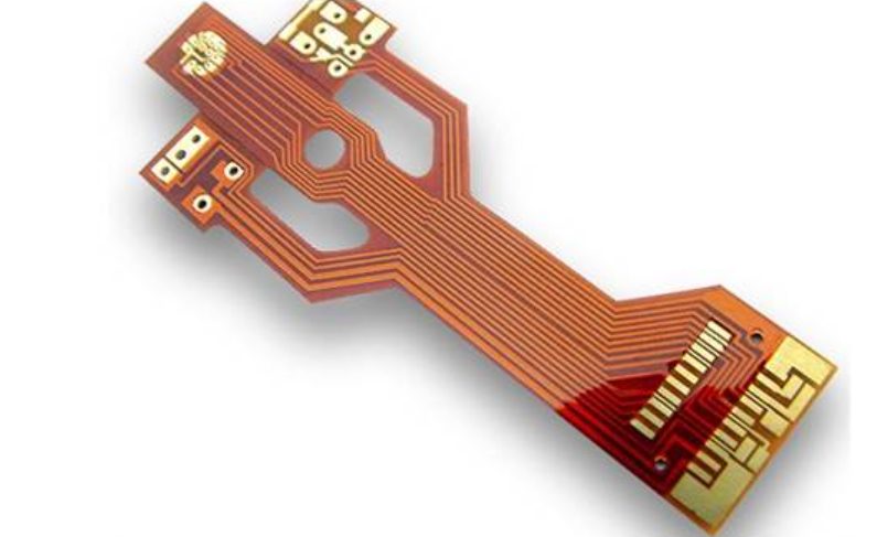
Flexible PCBs are a type of printed circuit board made from flexible materials, such as polyimide or polyester, allowing them to bend, twist, and fold without compromising electrical performance. Unlike traditional rigid PCBs built on hard substrates, flexible PCBs are designed for applications where space, weight, and movement are critical factors. In modern electronics, flexible PCB fabrication plays an essential role in industries like wearables, medical devices, and aerospace, where compactness, durability, and adaptability are required. These circuits enable devices to fit into unconventional shapes and withstand repeated mechanical stress. The flexible PCB fabrication process involves key steps such as layout design, careful material selection, trace etching, precise layering, and final testing to ensure optimal performance and reliability. With the growing demand for smaller, lighter, and more versatile electronics, flexible PCB fabrication continues to be a cornerstone technology for the next generation of innovative devices.
Key Materials Used in Flexible PCB Fabrication
The materials chosen for flexible PCB fabrication are crucial in determining the performance, durability, and cost of the final product. Understanding these materials is essential for designing high-quality flexible circuit boards that meet the demands of modern electronic devices.
Polyimide (PI) and PET (Polyester) in Flexible PCB Fabrication
Polyimide (PI) is the most commonly used flexible substrate in flexible PCB fabrication due to its excellent thermal stability, mechanical properties, and resistance to harsh environments. PI can withstand high temperatures and provides superior flexibility, making it ideal for applications that require bending and twisting. On the other hand, PET (Polyester) is often used for lower-cost applications. While it is more affordable, PET is less durable and has a lower heat resistance than PI, making it suitable for less demanding use cases.
Copper Foil in Flexible PCB Fabrication
Copper foil is used in flexible PCB fabrication as the conductive material for creating electrical traces and connections. The copper foil is bonded to the flexible substrate and then etched to form the desired circuitry. The thickness of the copper foil is an important consideration because it affects the current-carrying capacity and the overall strength of the circuit. In flexible PCB designs, thinner copper foils are often used to maintain flexibility without compromising conductivity.
Adhesives in Flexible PCB Fabrication
Adhesives play a crucial role in flexible PCB fabrication by bonding the layers of the flexible substrate while ensuring that the flexibility of the board is maintained. Specialized adhesives are required to maintain the integrity of the circuits while providing flexibility. These adhesives must be durable and able to withstand the mechanical stresses of bending, twisting, and stretching without breaking down or losing adhesive properties.
Material Selection and Its Impact on Fabrication
The selection of materials in flexible PCB fabrication directly impacts the performance, flexibility, and cost of the final product. For example, Polyimide is an ideal choice for high-performance applications due to its superior durability and temperature resistance, but it comes at a higher cost. PET, while more affordable, may not perform as well under extreme conditions. The choice of material also affects the fabrication process, as different substrates and adhesives require specific processing techniques, such as temperature control during lamination and curing. Balancing cost, performance, and flexibility is key to selecting the right materials for a given application.
Step-by-Step Flexible PCB Fabrication Process
The process of flexible PCB fabrication involves several crucial steps, each of which plays a vital role in ensuring the final product is durable, functional, and suitable for the intended application. Here’s a detailed look at the key stages in flexible PCB fabrication.
Design and Layout
The flexible PCB fabrication process begins with designing the layout of the circuit. This step involves creating the electrical connections and overall circuit structure using specialized flex PCB design software. These tools allow designers to place components and traces, define vias, and ensure proper electrical paths. In this phase, flex PCB design guidelines are crucial. Key considerations include the bending radius, trace width, and trace spacing. For flexible circuits, it’s essential to design traces that can endure repeated bending without compromising performance. The bend radius determines how tightly the PCB can bend without causing mechanical stress or failure. Ensuring trace width and impedance control is critical to maintaining signal integrity, especially in high-frequency applications.
Flex PCB Design Guidelines
The layout design must also consider the material properties and limitations of flexible substrates. For example, flex PCB design guidelines often specify a minimum bend radius to avoid breaking the conductive traces. The trace width is determined based on the current load and the desired impedance, as improper trace width can lead to signal loss or circuit overheating. Additionally, controlling the impedance is critical to avoid reflections and signal degradation, particularly in high-speed digital circuits. These design guidelines help optimize both the electrical performance and mechanical durability of the flexible PCB.
Lamination and Layering
Once the design is complete, the next step in flexible PCB fabrication is lamination and layering. Flexible PCBs are often built in multi-layer configurations for increased functionality and compactness. During this stage, copper foils are laminated onto flexible substrates like Polyimide or PET, creating the conductive paths needed for the circuit. This process also involves bonding the layers together using specific adhesives that maintain flexibility while holding the layers securely. The flex PCB stackup refers to the arrangement of these layers, ensuring proper alignment and electrical performance. The precise control of layer thickness and alignment is essential for ensuring the circuit’s flexibility and performance under bending.
Etching and Patterning
After lamination, the flexible PCB fabrication process moves to etching and patterning. This step involves using a chemical or laser process to remove unwanted copper, leaving behind the desired electrical traces and patterns. The etching process must be precise to avoid errors that could cause electrical shorts or open circuits. Etching also includes patterning the circuit board to define areas for components and vias. This process ensures that the flexible circuit can carry the required signals while maintaining integrity during bending and stretching.
Cutting and Shaping
The final step in flexible PCB fabrication is cutting and shaping the board to fit its intended form factor. Once the electrical traces and components are patterned and secured, the PCB is cut to the required shape, whether it’s a simple rectangular board or a more complex shape tailored for specific applications like wearable electronics or foldable displays. During this phase, it is essential to consider the preparation for dynamic bending—ensuring that the PCB will function properly even as it moves or flexes over time. Cutting and shaping also prepare the PCB for final testing and assembly, where it will undergo rigorous checks for quality, flexibility, and electrical performance.
Each of these stages in flexible PCB fabrication plays a critical role in creating a reliable, high-performance circuit that can meet the demands of modern electronic devices. From the initial design to the final cutting and shaping, careful attention to detail ensures that the PCB will function optimally in its intended application.
Rigid-Flex PCB Fabrication
Rigid-flex PCBs are a hybrid design that combines both rigid and flexible sections into one integrated board. These boards offer the best of both worlds, providing the mechanical stability and robustness of rigid PCBs along with the flexibility and compactness of flexible PCBs. Flexible PCB fabrication is a critical aspect of rigid-flex PCB production, but the process also involves unique considerations to accommodate both rigid and flexible areas on the same board.
Rigid-Flex PCBs: A Hybrid Design
A rigid-flex PCB is a design that integrates rigid sections with flexible portions, allowing for a flexible circuit to connect components while maintaining areas that provide structural integrity. Rigid-flex designs are often used in applications that require both high durability and flexibility, such as aerospace, military, medical devices, and compact consumer electronics. The rigid sections provide stable mounting and support for components, while the flexible sections enable the PCB to bend and conform to tight spaces. The use of flexible PCB fabrication techniques for the flexible parts ensures that the rigid-flex board can endure mechanical stresses and maintain reliable electrical performance in motion or during installation.
Rigid-Flex PCB Design Guidelines
When designing a rigid-flex PCB, there are unique considerations that differ from traditional flexible PCB designs. The most critical element is managing the transition zones between the rigid and flexible areas. These transition zones must be designed carefully to ensure that stress on the flexible sections does not cause damage to the rigid parts, and vice versa. For example, the bend radius in these areas must be chosen with care, ensuring that the flexible portions can bend without breaking the rigid sections.
Rigid-flex PCB design guidelines also include considerations for stackup design, trace width, impedance control, and materials. These factors are vital for ensuring that the circuit functions as intended and that both rigid and flexible areas can withstand environmental and mechanical stress. The material selection for rigid-flex designs is also crucial, as the substrates and adhesives must support both flexibility in certain areas and the rigidity needed in others.
Fabrication Process for Rigid-Flex PCBs
The flexible PCB fabrication process for rigid-flex boards differs in several ways compared to purely flexible designs. First, rigid-flex PCBs require multiple layers of materials to be laminated together. In the fabrication of rigid-flex boards, flexible layers are bonded with rigid layers using adhesive materials that are designed to withstand the mechanical and thermal stresses during operation. The rigid sections typically use traditional FR4 (fiberglass-reinforced epoxy laminate), while the flexible sections use materials like Polyimide or PET, depending on the application.
The rigid-flex PCB fabrication process also involves additional steps, such as creating specific vias and ensuring proper alignment between the rigid and flexible areas. Special care must be taken during lamination to avoid warping, delamination, or failure of the adhesives used to bond the rigid and flexible portions. After lamination, the board goes through the usual etching and patterning process to define the electrical traces. Finally, the board is cut into its final shape, ensuring that the flexible areas can bend without damaging the rigid areas.
Rigid-flex PCB fabrication requires a combination of flexible PCB fabrication techniques and traditional rigid PCB manufacturing processes. The challenges lie in managing the transition between rigid and flexible zones, ensuring proper layer bonding, and maintaining the mechanical and electrical integrity of the final product. By carefully following rigid-flex PCB design guidelines, manufacturers can produce boards that offer the flexibility needed in compact and complex electronic devices without sacrificing the durability and stability of rigid PCBs.
Important Design Considerations for Flexible PCB Fabrication
When it comes to flexible PCB fabrication, careful attention must be paid to several critical design factors to ensure that the final product is reliable, durable, and performs as intended. Each consideration plays a role in preventing failures and optimizing performance, particularly in applications where flexibility and mechanical movement are key requirements. Here’s a closer look at some of the most important design considerations for flexible PCB fabrication.
Flex PCB Bending Radius
One of the most crucial aspects of flexible PCB fabrication is determining and managing the bending radius of the board. The bending radius is the minimum radius the flexible PCB can be bent without causing damage, such as cracking or breaking the conductive traces. A bending radius that is too tight can cause the PCB to fail, while one that is too loose may compromise the functionality of the device.
To calculate the correct bending radius, factors such as the material thickness, trace width, and copper foil thickness must be considered. Typically, manufacturers will provide guidelines that specify the minimum bend radius based on these factors. It’s important to account for the fact that frequent or excessive bending can result in wear and tear on the PCB, which can lead to failure over time. Therefore, understanding how to properly manage the bending radius is essential for ensuring long-term performance in applications like wearables, medical devices, and other flexible electronics.
Impedance Control and Signal Integrity
Ensuring proper impedance control is another key consideration in flexible PCB fabrication. Impedance is a measure of the resistance to the flow of electrical signals and is critical for high-frequency signal transmission. Inaccurate impedance control can lead to signal reflection, loss, or interference, which can degrade the performance of the circuit.
For flexible PCB fabrication, maintaining consistent impedance is challenging due to the inherent flexibility of the board. This can be addressed by carefully controlling the width and spacing of traces, the distance between traces and ground planes, and the choice of materials. Using a controlled impedance approach ensures that signals flow with minimal distortion, which is particularly important in high-speed circuits used in applications like data transmission, communication devices, and high-frequency electronics.
Shielding and EMI/EMC
Electromagnetic interference (EMI) and electromagnetic compatibility (EMC) are significant concerns in flexible PCB fabrication. Flexible circuits, because of their small form factor and ability to bend, are often used in environments where space is limited, which can increase the risk of interference from external sources or other components on the board.
To mitigate these issues, designers often incorporate shielding in flexible PCB fabrication. Shielding involves using conductive materials or metal foils to encase sensitive components or traces, thereby preventing external electromagnetic waves from affecting the signal integrity. Additionally, EMC strategies, including grounding and placement of components, are employed to ensure that the flexible PCB operates within the required electromagnetic standards. These measures help maintain performance and ensure compliance with regulations for electromagnetic emissions, which is crucial for industries such as telecommunications, medical devices, and automotive electronics.
Ground Planes and Controlled Impedance Traces
Ground planes and controlled impedance traces play a crucial role in maintaining signal integrity in flexible PCB fabrication. A ground plane serves as a reference point for electrical signals and helps provide a low-resistance path to the ground. It also acts as a shield to reduce noise and minimize EMI.
Controlled impedance traces are essential for high-speed or high-frequency circuits, as they ensure the signal maintains its integrity throughout the PCB. The impedance of these traces needs to be tightly controlled to prevent signal degradation, crosstalk, or reflections. In flexible PCB fabrication, maintaining a stable ground plane and controlled impedance is more challenging than in rigid PCBs due to the board’s ability to flex. However, through careful design, such as ensuring adequate trace width, proper spacing, and alignment of ground planes, designers can achieve stable and reliable signal transmission.
By carefully addressing these design considerations in flexible PCB fabrication, manufacturers can create PCBs that meet the rigorous demands of flexible and high-performance electronics. These considerations ensure the PCB’s reliability, functionality, and durability in a wide range of applications, from wearable technology to automotive and industrial systems.
Challenges in Flexible PCB Fabrication
The process of flexible PCB fabrication introduces a unique set of challenges that must be addressed during both design and manufacturing. Unlike traditional rigid boards, flexible PCBs must endure mechanical movement and harsh environmental conditions while maintaining electrical performance. Understanding these challenges is essential for engineers and manufacturers aiming to produce high-reliability flex circuits.
Mechanical Stress and Durability
One of the primary challenges in flexible PCB fabrication is managing mechanical stress. Flexible circuits are designed to bend, twist, or fold repeatedly during use, especially in dynamic applications like wearable devices or foldable electronics. This movement can introduce strain on the copper traces and substrate, potentially leading to cracking, delamination, or circuit failure over time.
To ensure durability, designers must implement appropriate bend radius calculations, reinforce critical areas with strain reliefs, and avoid placing vias or components in high-flex regions. Materials such as polyimide provide better mechanical endurance, but the layout and construction must still be optimized to prevent failure during repeated mechanical cycles.
Thermal Cycling and Vibration
Thermal cycling — the process of exposing the circuit to alternating high and low temperatures — can cause expansion and contraction in the materials used during flexible PCB fabrication. These cycles may weaken adhesive bonds, cause delamination, or affect the electrical properties of the circuit. Similarly, vibration can fatigue solder joints and interconnects, especially in aerospace, automotive, or industrial applications.
To mitigate these effects, flexible PCB fabrication must include rigorous reliability testing, such as thermal shock, dynamic flex testing, and vibration simulations. These tests validate that the design can withstand its intended operating environment, helping ensure product longevity.
Manufacturing Complexity and Cost
Another major challenge in flexible PCB fabrication is the increased complexity and cost compared to rigid PCB production. Flex PCBs require specialized materials like thin copper foils and high-performance substrates, as well as precise handling and tooling due to their fragile, bendable nature. Additionally, multi-layer flex or rigid-flex boards often involve complex lamination and imaging processes that demand skilled labor and advanced equipment.
The yield rates can be lower due to potential defects like layer misalignment, cracking during cutting, or warping during lamination. These factors contribute to higher production costs and longer lead times. Manufacturers must work closely with designers to optimize the fabrication process and balance cost with performance and reliability.
While flexible PCB fabrication offers numerous benefits in terms of space savings and design freedom, it also presents significant challenges in terms of mechanical, thermal, and economic factors. Addressing these challenges through careful design and close collaboration with experienced manufacturers is key to achieving successful and cost-effective outcomes.

