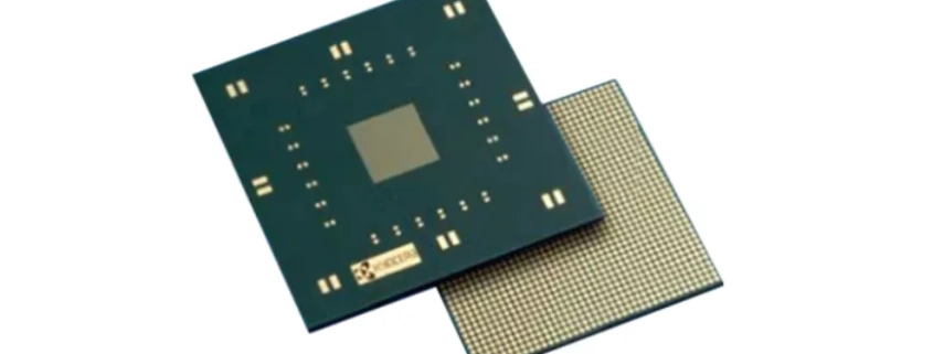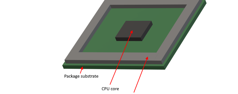
Integrated Circuit (IC) packaging plays a critical role in the performance and reliability of electronic devices. At its core, IC packaging involves enclosing the semiconductor material in a protective case that provides mechanical support, protects against physical damage and environmental hazards, and ensures efficient electrical connections to the circuit board. This packaging is essential not only for safeguarding the delicate IC components but also for enabling proper heat dissipation, which is crucial for maintaining optimal performance and longevity.
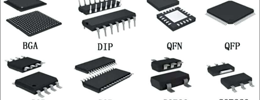
The purpose of this article is to provide a comprehensive overview of the most common IC package types and their specific applications. By understanding the different IC package types, from traditional Dual In-line Packages (DIP) to modern Ball Grid Arrays (BGA) and Chip Scale Packages (CSP), readers will gain insights into their unique characteristics, advantages, and ideal use cases. This knowledge is invaluable for engineers, designers, and enthusiasts looking to select the appropriate IC packages for their electronic projects.
阅读更多