
BGA Substrates Essentials: Materials and Design Considerations
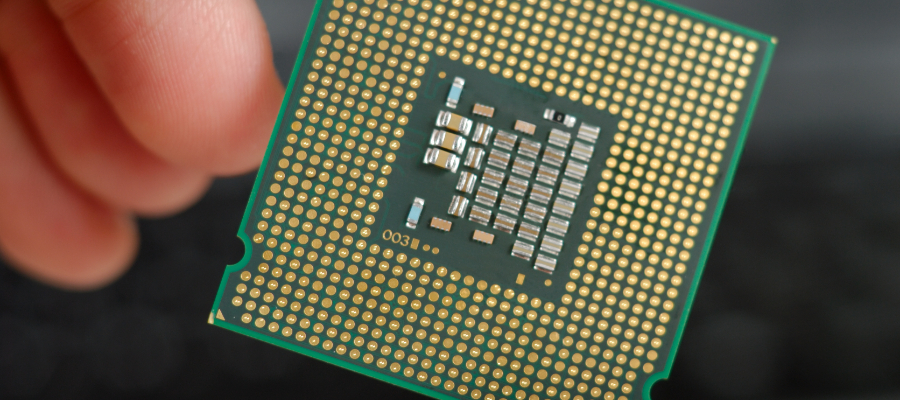
BGA (Ball Grid Array) packages are a crucial component in modern electronics, facilitating efficient electrical connections between integrated circuits and circuit boards. These packages feature an array of solder balls positioned beneath the chip, enhancing space utilization and enabling higher pin counts compared to traditional packaging methods. BGA’s significance lies in its ability to accommodate complex integrated circuits while offering improved thermal performance and signal integrity. Available in various types and sizes, including FC-BGA (Flip Chip BGA) and Micro BGA, these packages cater to diverse electronic applications, ranging from consumer electronics to telecommunications and automotive industries.
We are a professional Flip-chip BGA substrate manufacturer. We can produce various types of substrates, Ranging from 2 layers to 26 layers, and using ABF materials, Glass materials, Ceramic materials, BT materials, high-frequency materials, etc. Fast delivery, stable quality and reasonable price. If you have any design or production detail questions, you can contact us by email at any time and we are always ready to offer assistance. please send email to : PCB@ALCANTAPCB.COM
BGA Package Substrates: An Overview
Definition and Role of the Substrate in BGA Packages
The substrate in BGA packages serves as the foundation upon which the integrated circuit (IC) is mounted. It acts as a medium for connecting the IC to the rest of the system, typically via wire bonding or flip chip technology. The substrate provides mechanical support, electrical interconnections, and thermal dissipation for the IC.
Importance of Substrate Material Selection in BGA Design
The choice of substrate material significantly impacts the performance and reliability of the BGA package. Different substrates offer varying properties such as thermal conductivity, coefficient of thermal expansion (CTE), dielectric constant, and cost. Selecting the appropriate substrate material is crucial to ensure proper signal transmission, thermal management, and mechanical robustness of the BGA package.
Common Substrate Materials Used in BGA Packages
- FR-4 (Flame Retardant 4): FR-4 is a widely used substrate material due to its low cost and good electrical insulation properties. It consists of woven fiberglass cloth impregnated with an epoxy resin. While FR-4 offers satisfactory electrical performance for many applications, its thermal conductivity is relatively low, which may limit its suitability for high-power or high-frequency designs.
- Polyimide: Polyimide substrates, also known as Kapton, offer excellent thermal stability and mechanical strength. They are particularly suitable for applications requiring flexibility or high-temperature operation. Polyimide substrates are commonly used in space and aerospace applications, as well as in flexible circuits.
- BT (Bismaleimide Triazine): BT substrates offer superior thermal performance compared to FR-4, making them suitable for high-power and high-frequency applications. They have a lower CTE, which reduces the risk of thermal stress-induced failures. BT substrates are often used in advanced electronic devices such as high-speed routers, servers, and telecommunications equipment.
- Ceramic: Ceramic substrates, such as alumina (Al2O3) or aluminum nitride (AlN), offer excellent thermal conductivity and mechanical strength. They are preferred for applications requiring superior thermal management, such as power electronics and high-power RF amplifiers. Ceramic substrates also exhibit good dimensional stability over a wide temperature range.
Choosing the right substrate material involves considering factors such as electrical performance, thermal management requirements, cost constraints, and manufacturing processes. Each material has its advantages and limitations, and the selection should be tailored to meet the specific needs of the BGA package and its intended application.
Types of BGA Package Substrates
Comparison between FC-BGA (Flip Chip BGA) Substrate and Standard BGA Substrate
FC-BGA and standard BGA substrates represent two distinct approaches to packaging integrated circuits, each offering unique advantages and considerations.
- FC-BGA Substrate
- Introduction: FC-BGA, or Flip Chip BGA, involves directly mounting the IC chip upside down onto the substrate, with its active side facing the substrate. The electrical connections are made using tiny solder bumps, or balls, on the chip’s surface.
- Advantages:
- Shorter Electrical Paths: FC-BGA offers shorter electrical paths compared to standard BGA, leading to reduced signal propagation delays and improved electrical performance, especially in high-speed applications.
- Better Thermal Management: By placing the IC closer to the substrate, FC-BGA facilitates more efficient heat dissipation, enhancing thermal management capabilities.
- Higher I/O Density: FC-BGA allows for higher I/O (input/output) density, enabling the integration of more connections within a smaller footprint.
- Improved Signal Integrity: With reduced electrical path lengths and impedance mismatches, FC-BGA can enhance signal integrity and reduce electromagnetic interference.
- Standard BGA Substrate
- Introduction: Standard BGA packages involve mounting the IC chip with its active side facing up, typically using wire bonding or solder balls to connect it to the substrate.
- Advantages:
- Simplicity: Standard BGA packages are simpler to manufacture and assemble compared to FC-BGA, making them more cost-effective for certain applications.
- Robustness: The wire bonding method used in standard BGA packages provides a relatively robust electrical connection, suitable for applications with moderate electrical and thermal requirements.
- Versatility: Standard BGA packages are suitable for a wide range of applications, from low-power consumer electronics to industrial and automotive applications.
BGA Package Datasheets: Understanding Specifications
Key Information Provided in BGA Package Datasheets
BGA package datasheets contain essential information for understanding the characteristics and specifications of the package. Some key information typically provided includes:
- Package Dimensions: This includes the overall dimensions of the BGA package, including length, width, and height, as well as the pitch (spacing) between the solder balls.
- Electrical Specifications: These specifications cover parameters such as the number of I/O (input/output) pins, operating voltage, current ratings, and signal integrity characteristics like impedance and capacitance.
- Thermal Characteristics: Information on thermal resistance, power dissipation, and maximum operating temperature are crucial for assessing the package’s thermal performance and reliability.
- Mechanical Properties: This includes details on mechanical strength, shock resistance, and vibration tolerance, which are important for determining the package’s durability and suitability for various environments.
- Materials and Construction: BGA datasheets often specify the materials used in the substrate, solder balls, and encapsulation, providing insight into the package’s composition and manufacturing process.
- Reliability Data: Datasheets may include reliability information such as mean time between failures (MTBF), failure rates, and compliance with industry standards for reliability testing.
How to Interpret BGA Package Datasheets for Substrate-Related Information
When analyzing BGA package datasheets for substrate-related information, it’s essential to focus on the following aspects:
- Substrate Material: Look for details on the substrate material used in the package, such as FR-4, polyimide, or ceramic. Understanding the substrate material helps assess its thermal conductivity, electrical properties, and suitability for specific applications.
- Thermal Performance: Check for thermal characteristics such as thermal conductivity, thermal resistance, and maximum operating temperature. These parameters indicate the substrate’s ability to dissipate heat effectively and maintain reliable operation under various thermal conditions.
- Electrical Properties: Consider electrical specifications related to the substrate, such as dielectric constant, loss tangent, and impedance control. These parameters affect signal integrity and electrical performance, particularly in high-speed or high-frequency applications.
- Mechanical Strength: Assess mechanical properties like tensile strength, flexural modulus, and coefficient of thermal expansion (CTE) to evaluate the substrate’s mechanical robustness and reliability, especially in harsh operating environments.
- Compliance and Standards: Verify whether the substrate material meets industry standards and regulatory requirements for performance, reliability, and environmental sustainability.
By carefully examining these aspects of BGA package datasheets, engineers can make informed decisions regarding substrate selection and ensure optimal performance and reliability in their electronic designs.
BGA Packaging Process: Step-by-Step Guide
Overview of the BGA Packaging Process
The BGA packaging process involves several steps to assemble the integrated circuit (IC) chip onto the substrate and create reliable electrical connections between the chip and the substrate’s solder balls. Below is a brief overview of the typical BGA packaging process:
- Substrate Preparation: The substrate, typically made of materials like FR-4, polyimide, or ceramic, undergoes preparation steps such as cleaning, surface treatment, and application of solder mask to define the solder ball locations.
- Die Attach: The IC chip is mounted onto the substrate using adhesive materials. In the case of FC-BGA, the chip is attached with its active side facing downwards onto the substrate.
- Wire Bonding or Flip Chip Bonding: Depending on the BGA type, wire bonding or flip chip bonding techniques are used to create electrical connections between the IC chip and the substrate. Wire bonding involves connecting the chip’s bonding pads to the substrate using fine wires, while flip chip bonding utilizes solder bumps on the chip’s surface for direct attachment to the substrate.
- Encapsulation: The assembled IC chip and substrate are encapsulated with a protective material, such as epoxy resin, to secure the components and provide mechanical protection.
- Solder Ball Placement: Solder balls are placed onto the substrate’s pads using techniques such as solder ball placement machines or stencil printing.
- Reflow Soldering: The assembly undergoes reflow soldering, where it is heated to melt the solder balls, creating reliable electrical connections between the substrate and the IC chip.
- Testing and Inspection: The completed BGA package undergoes testing and inspection processes to ensure functionality, electrical continuity, and reliability.
Detailed Explanation of Substrate Attachment and Ball Placement
- Substrate Attachment: In the case of FC-BGA, the substrate attachment involves mounting the IC chip onto the substrate with its active side facing downwards. This process typically uses adhesive materials to secure the chip in place.
- Ball Placement: Solder balls are placed onto the substrate’s pads using precision equipment such as solder ball placement machines or stencil printing. The placement of solder balls is crucial for ensuring proper alignment and electrical connectivity between the IC chip and the substrate.
- Stencil Printing: Stencil printing is a common method for applying solder paste onto the substrate’s pads before solder ball placement. A stencil with openings corresponding to the pad locations is positioned over the substrate, and solder paste is applied through the stencil openings using a squeegee.
- Solder Ball Placement Machine: Solder ball placement machines use automated processes to accurately position solder balls onto the substrate’s pads. The machine picks up individual solder balls from a supply source and precisely places them onto the designated pad locations on the substrate.
- Alignment and Inspection: After solder ball placement, the assembly undergoes alignment and inspection processes to ensure the solder balls are properly aligned with the substrate’s pads. Any misalignment or defects are corrected before proceeding to the reflow soldering step.
- Reflow Soldering: During reflow soldering, the entire assembly is heated to a specific temperature, causing the solder balls to melt and form reliable electrical connections between the substrate and the IC chip. The assembly is then cooled to solidify the solder joints, completing the BGA packaging process.
By following these steps meticulously, manufacturers can produce BGA packages with high-quality electrical connections and reliable performance, meeting the demands of various electronic applications.
BGA Balls: Composition and Function
Composition of BGA Balls
BGA (Ball Grid Array) balls, also known as solder balls, are critical components of BGA packages, facilitating the electrical connections between the integrated circuit (IC) chip and the substrate. These solder balls are typically made of tin-based alloys, with lead-based alloys being less common due to environmental concerns. The composition of BGA balls may vary depending on factors such as the application requirements, manufacturing process, and environmental regulations.
Common compositions of BGA balls include:
- Tin-Lead (Sn-Pb) Alloys: Historically, solder balls were primarily composed of tin and lead alloys, such as eutectic (63% Sn, 37% Pb) or near-eutectic compositions. However, due to the implementation of regulations such as the Restriction of Hazardous Substances (RoHS), lead-free alternatives are now more prevalent.
- Lead-Free Alloys: Lead-free solder alloys, such as tin-silver-copper (Sn-Ag-Cu), tin-silver (Sn-Ag), or tin-copper (Sn-Cu), are widely used in modern BGA packages to comply with environmental regulations. These alloys offer comparable mechanical and electrical properties to traditional lead-based solder, while minimizing the environmental impact.
- Other Alloy Compositions: Some BGA packages may utilize specialized solder alloys tailored to specific application requirements, such as enhanced thermal conductivity, mechanical strength, or reliability. These alloys may incorporate elements like bismuth, antimony, or indium to achieve desired properties.
Role of BGA Balls in the Overall Functionality of the Package
BGA balls play several crucial roles in the functionality and reliability of BGA packages:
- Electrical Connectivity: BGA balls serve as the primary interface for electrical connections between the IC chip and the substrate. When the BGA package is mounted onto a circuit board, the solder balls establish contact with corresponding pads on the board, facilitating the transfer of electrical signals and power between the IC and the external circuitry.
- Mechanical Support: BGA balls provide mechanical support and anchorage for the IC chip, securing it to the substrate and preventing movement or detachment during operation. Proper soldering of the balls ensures structural integrity and reliability of the BGA package, particularly in applications subject to mechanical stress or vibration.
- Thermal Management: BGA balls contribute to the thermal management of the package by facilitating the dissipation of heat generated by the IC chip during operation. Efficient thermal conduction through the solder balls helps regulate the temperature of the IC and the surrounding components, mitigating the risk of overheating and prolonging device lifespan.
- Compliance and Reliability: BGA balls must meet stringent reliability standards to ensure long-term performance and compliance with industry regulations. Proper selection of solder alloys and meticulous manufacturing processes are essential to minimize the risk of defects such as solder joint cracking, solder ball bridging, or solder ball detachment, which can compromise the functionality and reliability of BGA packages.
BGA balls are integral components of BGA packages, providing essential electrical, mechanical, thermal, and reliability functions that are vital for the performance and longevity of electronic devices. The composition and quality of BGA balls are critical factors in ensuring the overall functionality and reliability of BGA packages in various applications.
Differences Between BGA and Micro BGA
Definition and Characteristics of Micro BGA Packages
Micro BGA (Micro Ball Grid Array) packages are a variation of traditional BGA packages, designed to accommodate smaller dimensions and higher pin densities. They are commonly used in applications where space constraints are critical, such as mobile devices, wearable electronics, and miniature sensors. Micro BGA packages typically feature a smaller overall size and pitch (spacing between solder balls) compared to standard BGA packages. Additionally, micro BGA packages often utilize finer pitch sizes, allowing for a higher density of solder balls and a greater number of I/O (input/output) connections within a compact footprint. Due to their miniaturized form factor, micro BGA packages require advanced manufacturing techniques and precise assembly processes to achieve reliable electrical connections and thermal performance.
Key Differences Between BGA and Micro BGA Packages
- Size and Pitch: One of the primary differences between BGA and micro BGA packages is their size and pitch. Micro BGA packages are significantly smaller in overall dimensions and have finer pitch sizes compared to standard BGA packages. This allows for a higher density of solder balls and a greater number of I/O connections in micro BGA packages, making them suitable for applications requiring miniaturization.
- Application: BGA packages are commonly used in various electronic devices and systems, ranging from consumer electronics to industrial applications. In contrast, micro BGA packages are specifically designed for applications where space constraints are critical, such as portable devices, embedded systems, and miniature sensors.
- Manufacturing Complexity: Due to their smaller size and finer pitch, micro BGA packages require more advanced manufacturing techniques and precise assembly processes compared to standard BGA packages. Specialized equipment and handling procedures are often necessary to ensure the accurate placement and soldering of solder balls in micro BGA packages, adding to the complexity and cost of manufacturing.
- Thermal Considerations: Micro BGA packages may present greater challenges in thermal management compared to standard BGA packages due to their smaller size and higher component density. Effective thermal design, including proper heat sinking and thermal vias, is essential to mitigate the risk of overheating and ensure reliable operation of micro BGA packages in high-temperature environments.
- Cost: The manufacturing complexity and specialized equipment required for micro BGA packages may result in higher production costs compared to standard BGA packages. However, the benefits of miniaturization and increased functionality in space-constrained applications often justify the investment in micro BGA technology.
While both BGA and micro BGA packages offer advantages in terms of electrical performance and reliability, their differences in size, pitch, application, manufacturing complexity, thermal considerations, and cost make each type suitable for specific use cases and design requirements. Understanding these differences is essential for selecting the most appropriate packaging solution for a given electronic design.
Popular BGA Package Sizes
Overview of Common BGA Package Sizes and Their Applications
BGA (Ball Grid Array) packages are available in a variety of sizes to accommodate different application requirements. Here’s an overview of some common BGA package sizes and their typical applications:
- 15mm x 15mm to 45mm x 45mm: These mid-size BGA packages are commonly used in a wide range of applications, including consumer electronics (such as smartphones, tablets, and laptops), networking equipment, automotive electronics, and industrial controllers. They offer a balance between size, pin density, and thermal performance, making them suitable for various electronic devices and systems.
- 5mm x 5mm to 10mm x 10mm: These smaller BGA packages, often referred to as micro BGA or ultra-fine pitch BGA, are utilized in applications where space constraints are critical, such as wearable devices, IoT (Internet of Things) sensors, embedded systems, and medical devices. Despite their compact size, they offer high pin densities and reliable electrical connections, enabling advanced functionality in miniaturized designs.
- 45mm x 45mm and larger: Larger BGA packages are commonly found in high-performance computing systems, servers, telecommunications infrastructure, and high-end networking equipment. These packages typically feature a higher pin count and are designed to accommodate complex integrated circuits with advanced functionalities, such as multicore processors, high-speed interfaces, and memory modules.
Largest BGA Package Available in the Market
The largest BGA packages available in the market are typically used in specialized applications requiring extensive I/O capabilities, high-power handling, and robust thermal management. While specific dimensions may vary depending on the manufacturer and application, some of the largest BGA packages can exceed 100mm x 100mm in size and feature several thousand solder balls.
These large BGA packages are commonly employed in:
- High-performance computing systems and servers
- Network switches and routers
- Data storage devices
- Graphics processing units (GPUs) and accelerators
- Test and measurement equipment
- Aerospace and defense electronics
The size and pin density of these largest BGA packages allow for the integration of multiple complex components, such as large-scale integrated circuits (LSIs), field-programmable gate arrays (FPGAs), and system-on-chip (SoC) solutions. Additionally, their robust construction and advanced thermal management capabilities ensure reliable operation in demanding environments.
Overall, the availability of BGA packages in a wide range of sizes enables designers to choose the most suitable package size for their specific application requirements, whether it involves miniaturization, high performance, or extensive I/O capabilities.
FAQs About BGA Package Substrates
In BGA (Ball Grid Array) packaging, the substrate refers to the underlying material upon which the integrated circuit (IC) chip is mounted. It serves as a foundation for electrical connections and mechanical support, typically consisting of materials like FR-4, polyimide, or ceramic.
The BGA packaging process involves mounting the IC chip onto the substrate, creating electrical connections, and encapsulating the assembly. This process includes steps such as die attach, wire bonding or flip chip bonding, solder ball placement, reflow soldering, and testing.
BGA balls, also known as solder balls, are typically made of tin-based alloys, such as tin-silver-copper (Sn-Ag-Cu) or tin-lead (Sn-Pb) for legacy applications. These alloys ensure reliable electrical conductivity and mechanical integrity in BGA packages.
The main difference between BGA (Ball Grid Array) and micro BGA lies in their size and pin density. Micro BGA packages are smaller and have finer pitch sizes compared to standard BGA packages, making them suitable for applications where space constraints are critical. Additionally, micro BGA packages often require more advanced manufacturing techniques and precise assembly processes due to their miniaturized form factor.


发表评论
Want to join the discussion?Feel free to contribute!