
Substrate Semiconductor Packaging: Materials and Processes
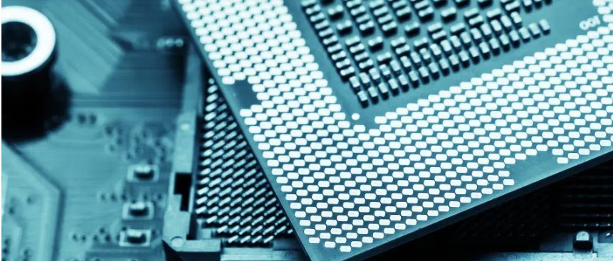
Semiconductor packaging plays a crucial role in protecting and enabling the functionality of integrated circuits (ICs). It involves encasing delicate semiconductor components to shield them from environmental factors, ensure electrical connections, and facilitate heat dissipation. The packaging process is vital for the reliability and performance of electronic devices, as it also includes provisions for power distribution and signal routing.
Within this context, substrates are a fundamental component. They serve as the foundation upon which ICs are mounted, providing both physical support and electrical interconnections. Substrates are critical in defining the package’s overall electrical performance, thermal management, and mechanical stability. As technology advances, the demands on substrates increase, requiring them to be more compact, efficient, and capable of supporting higher frequencies and power levels. This makes the choice of substrate materials and design a key consideration in the development of advanced semiconductor packages.
What is a Substrate in Semiconductor Packaging?
Definition and Explanation
In semiconductor packaging, a substrate is the foundational layer onto which semiconductor devices, such as integrated circuits (ICs), are mounted and connected. The substrate provides a stable base for the delicate silicon chips and serves as a bridge between the IC and the external environment. It is typically composed of various materials like organic laminates, ceramics, or metals, which are chosen based on the specific requirements of the device and its intended application.
Role and Significance in Semiconductor Devices
The substrate plays several critical roles in the functionality and performance of semiconductor devices:
- Mechanical Support: It provides structural integrity to the package, ensuring that the delicate silicon chip remains protected and intact throughout its lifecycle. This support is crucial during handling, assembly, and operation.
- Electrical Interconnections: The substrate contains intricate patterns of conductive traces that establish electrical connections between the IC and the external circuits. These interconnections are essential for signal transmission, power distribution, and ground connections, facilitating the IC’s integration into broader electronic systems.
- Thermal Management: As electronic devices become more powerful and compact, managing heat becomes a significant challenge. Substrates often incorporate materials with good thermal conductivity to dissipate heat generated by the ICs, preventing overheating and ensuring reliable performance.
- Packaging and Protection: Beyond mechanical support and electrical connections, substrates also contribute to the overall protection of the IC. They shield the chip from environmental factors such as moisture, dust, and mechanical stress, which can affect the device’s reliability and longevity.
- Integration and Miniaturization: As technology advances, there is a growing demand for smaller, more integrated devices. Substrates facilitate this by enabling the integration of various functions and components into a single package, reducing the size and weight of the final product.
The design and selection of substrates are crucial considerations in semiconductor packaging, directly impacting the device’s electrical performance, thermal efficiency, and overall reliability. As such, substrates are not just a passive support layer but a key component that influences the success of modern electronic devices.
Types of Packaging Substrates
In semiconductor packaging, the choice of substrate material is crucial as it influences the electrical, thermal, and mechanical properties of the device. The main types of packaging substrates include organic, ceramic, and flexible substrates, each offering unique advantages and suited for specific applications.
Organic Substrates
Overview: Organic substrates are widely used in semiconductor packaging due to their versatility and cost-effectiveness. They are typically made from epoxy resins reinforced with glass fibers, known as FR-4, or from bismaleimide triazine (BT) resins.
Characteristics:
- Electrical Performance: Organic substrates provide good electrical insulation and are suitable for high-density interconnects. They support fine-line circuitry, which is essential for modern high-performance devices.
- Thermal Management: While organic materials generally have lower thermal conductivity than ceramics, advancements in material science have led to improved thermal management solutions, including the integration of heat spreaders and thermal vias.
- Mechanical Properties: These substrates offer good mechanical strength and flexibility, making them ideal for various applications, including mobile devices and consumer electronics.
Applications: Organic substrates are commonly used in applications where cost and weight are critical factors, such as in smartphones, tablets, and other portable electronics.
Ceramic Substrates
Overview: Ceramic substrates are made from materials like alumina (Al₂O₃), aluminum nitride (AlN), or silicon carbide (SiC). These substrates are known for their excellent thermal and mechanical properties.
Characteristics:
- Thermal Management: Ceramic substrates have high thermal conductivity, making them ideal for applications that generate significant heat, such as power electronics and radio frequency (RF) devices.
- Electrical Insulation: They provide excellent electrical insulation and stability, which is crucial for high-frequency and high-power applications.
- Mechanical Strength: Ceramics are rigid and offer high mechanical strength, making them suitable for harsh environments and applications requiring durability.
Applications: Due to their properties, ceramic substrates are often used in aerospace, automotive, and industrial applications where reliability and performance are critical. They are also favored in high-frequency applications due to their low dielectric loss.
Flexible Substrates
Overview: Flexible substrates are made from materials like polyimide or other flexible polymers. They are used in applications requiring flexibility and the ability to conform to various shapes.
Characteristics:
- Flexibility: These substrates can bend and twist, making them ideal for wearable devices, flexible displays, and other applications where traditional rigid substrates are unsuitable.
- Lightweight: Flexible substrates are generally lighter than their rigid counterparts, contributing to the miniaturization and weight reduction of electronic devices.
- Thermal and Electrical Properties: While flexible substrates may not match the thermal and electrical performance of ceramic or high-end organic substrates, they are sufficient for applications that prioritize flexibility and low weight.
Applications: Flexible substrates are commonly used in flexible electronics, medical devices, and other applications where a lightweight and adaptable form factor is essential.
Each type of substrate—organic, ceramic, and flexible—offers distinct advantages and is selected based on the specific requirements of the semiconductor device and its intended application. The choice of substrate material significantly impacts the overall performance, cost, and reliability of the final product.
Package Substrate vs. PCB
In the realm of electronics, both package substrates and printed circuit boards (PCBs) play crucial roles in supporting and interconnecting electronic components. However, they serve different functions and are designed for distinct purposes within electronic systems.
Differences Between Package Substrates and Printed Circuit Boards (PCBs)
1. Purpose and Functionality:
- Package Substrates:
- Package substrates are specialized materials used in semiconductor packaging to provide a foundation for mounting integrated circuits (ICs). They offer electrical interconnections, mechanical support, and thermal management for the ICs, and serve as the interface between the chip and the larger electronic system.
- The primary function of package substrates is to protect the IC, facilitate signal and power distribution, and manage heat dissipation. They are designed to accommodate the miniaturization of components and support high-density interconnects.
- Printed Circuit Boards (PCBs):
- PCBs are used to mechanically support and electrically connect various electronic components using conductive pathways, tracks, or signal traces etched from copper sheets laminated onto a non-conductive substrate. PCBs serve as the backbone of electronic devices, providing the necessary connections and layout for the entire system.
- The main purpose of a PCB is to integrate multiple electronic components, such as resistors, capacitors, and ICs, into a cohesive system. PCBs enable the construction of complex circuits and are essential in nearly all electronic devices.
2. Design and Structure:
- Package Substrates:
- Typically smaller and more compact than PCBs, package substrates are designed to support a single or a few semiconductor chips. They may include features like bond pads, microvias, and fine-line wiring to facilitate the connection between the IC and external circuits.
- Package substrates are often layered structures, including a core substrate material and one or more layers of conductive traces. The materials used are selected for their thermal and electrical properties.
- Printed Circuit Boards (PCBs):
- PCBs vary widely in size and complexity, from simple single-layer boards to complex multi-layer designs. They are typically larger than package substrates and include various mounting and interconnection features for multiple components.
- PCBs consist of multiple layers of conductive and insulating materials. The number of layers can range from a single layer to more than 50 layers in advanced applications, providing a versatile platform for creating intricate circuits.
3. Materials and Manufacturing:
- Package Substrates:
- Materials used in package substrates include organic laminates (such as FR-4 and BT resin), ceramics, and sometimes metals. The choice of material depends on the specific requirements of the semiconductor device, including electrical performance, thermal conductivity, and mechanical properties.
- Manufacturing processes for package substrates often involve advanced techniques such as photolithography, electroplating, and etching, which allow for fine-line features and high-density interconnects.
- Printed Circuit Boards (PCBs):
- PCBs are typically made from fiberglass-reinforced epoxy resin (FR-4) or other composite materials. The conductive layers are usually made of copper, which is laminated onto the substrate and patterned to form the circuit traces.
- The PCB manufacturing process includes steps like design, etching, drilling, plating, and solder mask application. PCBs can be customized for a wide range of applications, from simple consumer electronics to complex industrial systems.
Specific Applications and Use Cases
Package Substrates:
- Semiconductor Packaging: Used primarily in the packaging of ICs, including processors, memory chips, and other semiconductor devices. Package substrates are critical in high-performance computing, mobile devices, and communication systems.
- Advanced Packaging Technologies: Key component in advanced packaging techniques such as flip-chip, chip-scale packages (CSP), and ball grid arrays (BGA), which require precise electrical and thermal performance.
Printed Circuit Boards (PCBs):
- Consumer Electronics: Widely used in consumer electronics like smartphones, tablets, televisions, and home appliances, where they provide the foundational structure for the entire electronic system.
- Industrial and Automotive Applications: Essential in industrial control systems, automotive electronics, and aerospace technology, where reliability and durability are paramount.
- Prototyping and Development: PCBs are commonly used in prototyping and development phases of electronic product design, allowing engineers to test and refine their circuits before mass production.
Understanding the differences and specific applications of package substrates and PCBs is crucial for designing efficient and reliable electronic systems. Both components are integral to the functioning of modern electronics, each serving unique roles within the overall architecture.
Materials Used for Packaging Substrates
The choice of material for packaging substrates is critical as it directly impacts the electrical performance, thermal management, and mechanical stability of semiconductor devices. Several materials are commonly used, each offering distinct properties and advantages. Below are some of the most prevalent materials:
1. FR-4
Overview:
FR-4 is a widely used composite material made from woven fiberglass cloth with an epoxy resin binder. It is known for its excellent balance of properties, making it a standard choice in both PCBs and package substrates.
Properties:
- Electrical Insulation: FR-4 offers good dielectric properties, making it suitable for insulating and supporting electrical circuitry.
- Mechanical Strength: It provides robust mechanical stability, which is essential for protecting sensitive semiconductor components.
- Thermal Resistance: While not as high as ceramic materials, FR-4 has adequate thermal resistance for many applications, with the ability to operate at temperatures up to approximately 130°C.
Advantages:
- Cost-Effectiveness: FR-4 is relatively inexpensive compared to other substrate materials, which makes it a popular choice for cost-sensitive applications.
- Versatility: It is versatile and can be used in various electronic devices, from consumer electronics to industrial equipment.
2. BT Resin (Bismaleimide Triazine Resin)
Overview:
BT resin is a type of thermosetting polymer used in high-performance packaging substrates. It is often combined with glass fibers to form a composite material.
Properties:
- High Glass Transition Temperature (Tg): BT resin has a high Tg, typically above 170°C, which allows it to maintain its mechanical and electrical properties at elevated temperatures.
- Low Dielectric Constant: This property is crucial for high-frequency applications, as it helps to reduce signal loss and crosstalk.
- Good Thermal Conductivity: BT resin substrates often incorporate fillers to enhance thermal conductivity, making them suitable for applications requiring effective heat dissipation.
Advantages:
- High Reliability: BT resin substrates are known for their reliability in demanding environments, making them ideal for telecommunications and automotive applications.
- Improved Signal Integrity: The low dielectric constant and loss factor contribute to better signal integrity, essential for high-speed electronic devices.
3. Ceramic Materials
Overview:
Ceramic substrates, such as alumina (Al₂O₃), aluminum nitride (AlN), and silicon carbide (SiC), are used in applications that require high thermal conductivity, electrical insulation, and mechanical strength.
Properties:
- High Thermal Conductivity: Ceramic materials like AlN and SiC offer superior thermal conductivity, making them ideal for high-power and high-temperature applications.
- Excellent Electrical Insulation: Ceramics provide excellent dielectric properties, which are crucial for maintaining electrical isolation in electronic circuits.
- Mechanical Robustness: Ceramics are inherently strong and resistant to wear and corrosion, which makes them suitable for harsh environments.
Advantages:
- Thermal Management: Their high thermal conductivity allows efficient heat dissipation, protecting semiconductor devices from thermal degradation.
- Durability: Ceramics are durable and reliable, often used in aerospace, military, and industrial applications where performance and longevity are critical.
4. Polyimide
Overview:
Polyimide is a flexible polymer material known for its high thermal stability and excellent mechanical properties. It is often used in flexible substrates and applications requiring a lightweight and adaptable material.
Properties:
- High Thermal Stability: Polyimide can withstand high temperatures, typically up to 300°C, without losing its properties, making it suitable for high-temperature applications.
- Flexibility: This material is highly flexible, allowing it to bend and conform to various shapes, which is essential for flexible and wearable electronics.
- Good Dielectric Properties: Polyimide offers good electrical insulation, crucial for maintaining circuit integrity.
Advantages:
- Lightweight: Polyimide substrates are lightweight, which is beneficial in applications where weight reduction is critical, such as aerospace and portable electronics.
- Chemical Resistance: Polyimide is resistant to chemicals and solvents, making it durable in chemically harsh environments.
Each of these materials—FR-4, BT resin, ceramics, and polyimide—offers unique advantages that make them suitable for specific applications. The selection of substrate material depends on the requirements of the semiconductor device, including operating temperature, electrical performance, thermal management, and mechanical durability. As technology advances, the development of new materials and composites continues to enhance the capabilities and applications of semiconductor packaging substrates.
Substrate Manufacturing Process
The manufacturing process for packaging substrates is a complex sequence of steps that involves precise engineering and advanced technologies. This process ensures that substrates meet the necessary specifications for electrical, thermal, and mechanical performance. Below are the key steps and advanced techniques involved in substrate manufacturing:
Key Steps in Substrate Manufacturing
- Material Preparation:
- The first step involves selecting and preparing the raw materials, such as fiberglass cloth for organic substrates or ceramic powders for ceramic substrates. These materials are chosen based on the desired electrical and thermal properties of the final substrate.
- Lamination:
- In the case of organic substrates, layers of fiberglass cloth are impregnated with epoxy resin and then laminated under heat and pressure to form a solid sheet. For ceramic substrates, ceramic powders are mixed with binders and cast into sheets, which are then laminated and sintered to achieve the desired thickness and density.
- Circuit Patterning:
- Once the base substrate is prepared, a photoresist is applied to its surface. This resist is patterned using photolithography, where ultraviolet (UV) light is used to transfer the circuit design onto the substrate. The exposed areas are developed and etched away to create the fine-line circuitry necessary for connecting semiconductor devices.
- Plating:
- After etching, the substrate undergoes plating processes, such as copper plating, to build up the conductive traces and pads. This step is crucial for ensuring reliable electrical connections and often involves electroplating or electroless plating techniques.
- Drilling and Via Formation:
- Vias, or vertical interconnect access, are created by drilling holes through the substrate layers. These vias are then plated to provide electrical connections between different layers of the substrate. The drilling can be performed using mechanical drills, laser drilling, or other advanced techniques depending on the precision required.
- Solder Mask and Surface Finish:
- A solder mask is applied over the circuit traces to protect against oxidation and prevent solder bridging during component assembly. The surface finish, such as HASL (Hot Air Solder Leveling), ENIG (Electroless Nickel Immersion Gold), or OSP (Organic Solderability Preservative), is applied to ensure good solderability and protect the exposed copper.
- Testing and Inspection:
- The finished substrates undergo rigorous testing and inspection to verify their electrical and mechanical properties. This includes continuity testing, impedance measurement, and visual inspection for defects such as scratches, misalignments, or voids.
Advanced Technologies and Techniques
- High-Density Interconnects (HDI):
- HDI technology involves the use of microvias, blind and buried vias, and fine-line circuitry to achieve higher wiring density and miniaturization. This technique is essential for advanced electronic devices that require complex interconnections in a compact form factor.
- Embedded Components:
- Advanced substrates can integrate passive components, such as resistors and capacitors, within the substrate layers. This embedding technique reduces the size of the final package and improves electrical performance by minimizing parasitic effects.
- Advanced Plating Techniques:
- Techniques such as additive manufacturing and selective plating allow for more precise control over the thickness and composition of conductive layers. These methods enhance the electrical performance and reliability of the substrates.
- Material Innovations:
- New materials, such as low-loss laminates, high-Tg resins, and advanced ceramics, are being developed to improve the thermal and electrical properties of substrates. These materials enable substrates to operate at higher frequencies and temperatures.
- Laser Direct Imaging (LDI):
- LDI is an advanced photolithography technique that uses laser beams to directly write circuit patterns onto the substrate. This method offers higher precision and flexibility compared to traditional mask-based photolithography, making it ideal for fine-pitch and high-density designs.
- Advanced Inspection and Testing:
- Automated Optical Inspection (AOI) and X-ray inspection are used to detect defects that are not visible to the naked eye. These advanced inspection techniques ensure the quality and reliability of the substrates, particularly in high-performance and safety-critical applications.
The substrate manufacturing process is continuously evolving, driven by the demand for smaller, faster, and more reliable electronic devices. Advanced technologies and materials are enabling the production of substrates with superior performance characteristics, supporting the ongoing innovation in semiconductor packaging and electronics.
Major Semiconductor Substrate Manufacturers
The semiconductor substrate market is dominated by a few key players who lead in innovation, production capacity, and technology development. These companies provide a wide range of substrate materials and solutions that are critical to the performance and advancement of semiconductor devices. Below is an overview of some of the leading companies in the industry and their contributions:
1. Ibiden Co., Ltd.
Overview:
Ibiden, a Japanese multinational corporation, is a major player in the semiconductor substrate industry, known for its advanced technology and high-quality products. The company specializes in organic substrates, including high-density interconnect (HDI) substrates and build-up substrates.
Products and Innovations:
- Flip-Chip Ball Grid Array (FC-BGA) Substrates: Ibiden is renowned for its FC-BGA substrates, which are used in high-performance computing and communication devices. These substrates offer fine pitch, high wiring density, and excellent thermal performance.
- Environmentally Friendly Materials: The company emphasizes the development of environmentally friendly materials, incorporating lead-free and halogen-free technologies to meet global environmental standards.
- Advanced Interconnect Solutions: Ibiden invests heavily in R&D to develop advanced interconnect solutions that support miniaturization and higher performance in semiconductor devices.
2. Shinko Electric Industries Co., Ltd.
Overview:
Shinko Electric, also based in Japan, is a leader in the manufacturing of semiconductor packaging substrates and advanced interconnect technologies. The company offers a wide range of products, including organic and ceramic substrates.
Products and Innovations:
- Build-Up Substrates: Shinko Electric is known for its high-density build-up substrates, which are essential for advanced packaging technologies like System in Package (SiP) and 3D packaging.
- Ceramic Substrates: The company provides high-performance ceramic substrates that offer superior thermal conductivity and electrical insulation, catering to applications in power electronics and RF devices.
- Innovative Packaging Solutions: Shinko is at the forefront of developing innovative packaging solutions, including fan-out wafer-level packaging (FOWLP) and chip-scale packages (CSPs), aimed at enhancing device performance and reducing size.
3. Unimicron Technology Corporation
Overview:
Unimicron, headquartered in Taiwan, is one of the world’s largest PCB and IC substrate manufacturers. The company has a strong presence in both the consumer electronics and automotive sectors, providing substrates that support a wide range of applications.
Products and Innovations:
- High-Density Interconnect (HDI) PCBs: Unimicron produces advanced HDI PCBs that are used in smartphones, tablets, and other compact electronic devices, offering high wiring density and fine-line capabilities.
- Substrate-Like PCBs (SLP): The company has pioneered the development of SLPs, which combine the features of traditional PCBs and IC substrates, allowing for even greater miniaturization and integration.
- Sustainability Initiatives: Unimicron is committed to sustainable manufacturing practices, including reducing hazardous substances and implementing energy-efficient processes.
4. ASE Technology Holding Co., Ltd.
Overview:
ASE Technology, based in Taiwan, is a global leader in semiconductor packaging and testing services. The company is a major supplier of advanced packaging substrates, including those used in system-in-package (SiP) and advanced IC packaging.
Products and Innovations:
- Advanced Packaging Substrates: ASE provides a range of substrates for advanced packaging technologies, including flip-chip, wafer-level packaging (WLP), and 3D integrated circuits (3D ICs).
- Thermal Management Solutions: The company develops substrates with enhanced thermal management features, which are critical for high-power and high-frequency applications.
- Global Manufacturing Footprint: With facilities around the world, ASE has a robust manufacturing network that supports a diverse range of industries, from consumer electronics to automotive and aerospace.
5. TTM Technologies, Inc.
Overview:
TTM Technologies, an American company, is a leading global provider of time-critical and technologically advanced PCBs and substrate solutions. The company serves a broad range of markets, including aerospace, defense, telecommunications, and industrial applications.
Products and Innovations:
- High-Performance PCBs: TTM specializes in producing high-performance PCBs, including those for RF and microwave applications, which require precise impedance control and low signal loss.
- Advanced Substrate Solutions: The company offers advanced substrate solutions, such as substrate-like PCBs (SLPs) and IC substrates, which support the latest semiconductor technologies.
- Focus on Innovation: TTM is known for its continuous investment in research and development, driving innovations in materials, manufacturing processes, and product capabilities.
These companies are at the forefront of the semiconductor substrate industry, driving advancements in materials, processes, and technologies that enable the production of smaller, faster, and more efficient electronic devices. Their innovations are critical in meeting the growing demand for high-performance computing, telecommunications, automotive electronics, and other applications.
Applications of Packaging Substrates in Chips
Packaging substrates are a fundamental component in semiconductor devices, serving as the interface between the silicon die and the external circuitry. They provide mechanical support, electrical interconnections, and thermal management. The choice and design of packaging substrates significantly influence the performance, reliability, and form factor of semiconductor devices. Below are detailed use cases and the impact of packaging substrates on various types of semiconductor devices:
Use Cases in Different Types of Semiconductor Devices
- Microprocessors and High-Performance CPUs:
Applications:
- Packaging substrates in microprocessors and CPUs are crucial for managing the high pin count and complex interconnections required for advanced computing tasks. They support technologies like flip-chip and multi-chip modules (MCMs), which are essential for integrating multiple functions on a single chip.
Impact on Performance and Reliability:
- Electrical Performance: High-performance CPUs require substrates with low electrical resistance and high signal integrity to support fast data transmission and minimize latency.
- Thermal Management: Effective thermal management is critical in CPUs to prevent overheating and maintain optimal performance. Substrates with high thermal conductivity, such as those made from BT resin or ceramic, are often used.
- Reliability: Advanced substrate materials and designs enhance the mechanical stability and durability of the package, reducing the risk of failure due to thermal cycling or mechanical stress.
- Memory Devices (DRAM, Flash Memory):
Applications:
- Memory devices use packaging substrates to connect memory chips to the system board. These substrates are designed to handle high data rates and large amounts of data transfer between the memory chips and the processor.
Impact on Performance and Reliability:
- Signal Integrity: Substrates for memory devices must have excellent signal integrity to ensure reliable data transmission, which is critical for maintaining the performance of high-speed memory modules.
- Compactness: With the trend toward miniaturization, substrates help in reducing the overall package size while maintaining high-density interconnections.
- Cost-Effectiveness: Memory devices are produced in large volumes, and cost-effective substrate materials like FR-4 are often used, balanced with the need for reliable performance.
- Power Electronics:
Applications:
- Power electronics, such as power management integrated circuits (PMICs) and power transistors, use substrates that can handle high currents and voltages. These devices are used in applications ranging from consumer electronics to automotive and industrial systems.
Impact on Performance and Reliability:
- Thermal Performance: Power electronics generate significant heat, requiring substrates with high thermal conductivity, such as aluminum nitride (AlN) or copper, to dissipate heat efficiently and maintain device reliability.
- Electrical Insulation: High dielectric strength is necessary to prevent electrical breakdown in power devices, which substrates like ceramics provide.
- Durability: Substrates in power electronics must be robust to withstand thermal cycling and mechanical stresses, ensuring long-term reliability in harsh operating conditions.
- Radio Frequency (RF) and Microwave Devices:
Applications:
- RF and microwave devices, used in communication systems and radar, require substrates that can support high-frequency signals with minimal loss. These devices include RF amplifiers, mixers, and oscillators.
Impact on Performance and Reliability:
- Dielectric Properties: Substrates for RF applications need low dielectric constant and low loss tangent materials to minimize signal attenuation and ensure high-frequency performance.
- Thermal Management: As RF devices can generate substantial heat, substrates with good thermal properties are essential to prevent performance degradation.
- Signal Integrity: The choice of substrate material and design directly impacts the impedance matching and signal integrity, crucial for the accurate transmission and reception of signals.
- Optoelectronic Devices:
Applications:
- Optoelectronic devices, such as LEDs, photodiodes, and laser diodes, rely on packaging substrates for efficient thermal management and electrical interconnections. These devices are commonly used in displays, communication systems, and sensors.
Impact on Performance and Reliability:
- Thermal Conductivity: High thermal conductivity substrates, often ceramics, are used to manage the heat generated by optoelectronic devices, which is critical for maintaining performance and extending lifespan.
- Optical Clarity: For devices like LEDs, substrates must also accommodate optical elements, necessitating materials that do not interfere with light emission or transmission.
- Durability: Optoelectronic devices often operate in varying environmental conditions, requiring substrates that are resistant to thermal and mechanical stresses.
- System-in-Package (SiP) and Multi-Chip Modules (MCMs):
Applications:
- SiP and MCM technologies integrate multiple semiconductor dies and passive components into a single package, relying heavily on advanced packaging substrates to support complex interconnections and efficient heat dissipation.
Impact on Performance and Reliability:
- Integration Density: Advanced substrates enable high integration density, reducing the overall footprint of electronic systems and supporting miniaturization trends.
- Thermal and Electrical Performance: The substrates used in SiP and MCMs must provide excellent thermal and electrical performance to ensure reliable operation of densely packed components.
- Customizability: The ability to customize substrate designs allows for optimized layouts that can accommodate various die sizes, configurations, and interconnection needs.
Differences Between Substrate and Package
In semiconductor technology, “substrate” and “package” are terms that often come up, and while they are related, they serve distinct roles in the assembly and function of electronic devices. Understanding the differences between these two components and how they work together can help clarify their respective functions and contributions to the performance and reliability of semiconductor devices.
Detailed Comparison
- Definition and Purpose:
- Substrate:
- Definition: A substrate in semiconductor packaging refers to the base material that provides the foundational support for the semiconductor chip and its interconnections. It is the layer or layers on which the semiconductor die is mounted and connected to external circuitry.
- Purpose: The substrate’s primary functions include providing mechanical support, facilitating electrical connections between the semiconductor die and external circuits, and managing thermal dissipation. It acts as the medium through which electrical signals and power are transmitted from the chip to the outside world.
- Package:
- Definition: A package refers to the complete enclosure and assembly that houses the semiconductor chip. It includes the substrate but also encompasses additional elements such as the lid or encapsulation material, which protect the chip from environmental damage and physical stress.
- Purpose: The package provides protection to the semiconductor die from physical, chemical, and thermal hazards. It also ensures that the chip is properly connected to the printed circuit board (PCB) or system through various bonding and mounting technologies. The package is crucial for maintaining the chip’s integrity and ensuring reliable operation within the electronic system.
- Structure and Composition:
- Substrate:
- Composition: The substrate is typically made from materials like organic laminates (e.g., FR-4, BT resin), ceramics (e.g., alumina, aluminum nitride), or flexible materials (e.g., polyimide). It may consist of multiple layers, including conductive traces and insulating layers.
- Structure: It features conductive pathways (traces), vias, and bond pads designed to establish electrical connections between the die and external pins or solder balls. The substrate may also include thermal management features such as heat spreaders or thermal vias.
- Package:
- Composition: The package encompasses the substrate and additional components such as the encapsulation material (e.g., epoxy mold compound), heat spreaders, and protective lids. The encapsulation material protects the chip from moisture, dust, and mechanical damage.
- Structure: The package includes the substrate, the encapsulation that surrounds the die, and external connectors such as pins, balls, or lands that interface with the PCB or system. The package design also incorporates features for thermal dissipation and mechanical stability.
- Function and Role:
- Substrate:
- Function: The substrate’s main function is to serve as the base for mounting the semiconductor die and to provide electrical and thermal pathways between the die and the external system. It supports the chip’s electrical interconnections and helps in managing heat generated during operation.
- Role: In the context of semiconductor packaging, the substrate is a critical component that influences the electrical performance, thermal management, and mechanical stability of the device. It enables high-density interconnections and contributes to the overall reliability of the semiconductor device.
- Package:
- Function: The package’s primary function is to protect the semiconductor die from external factors, ensure reliable electrical connections to the PCB, and manage heat dissipation. It provides the final form and interfaces for the semiconductor device, enabling its integration into electronic systems.
- Role: The package plays a crucial role in the protection, thermal management, and integration of the semiconductor chip. It ensures that the die remains functional and protected while facilitating its connection to the broader electronic system.
How They Work Together in Semiconductor Devices
- Integration:
- The substrate and package work together to ensure that the semiconductor chip is effectively mounted, connected, and protected. The substrate provides the necessary electrical and thermal interfaces for the chip, while the package encompasses the substrate and the chip to protect them from environmental damage and mechanical stress.
- Electrical Connectivity:
- The substrate contains the circuitry and interconnections required to connect the semiconductor die to the package’s external pins or solder balls. This allows electrical signals and power to flow between the chip and the PCB or other components in the system.
- Thermal Management:
- Effective thermal management is achieved through the combination of the substrate and package. The substrate often includes thermal vias or heat spreaders to dissipate heat away from the die, while the package may include additional features such as heat sinks or thermal pads to further manage heat.
- Mechanical Protection:
- The package provides mechanical protection to the semiconductor die and substrate. Encapsulation materials and protective lids shield the chip from physical damage, moisture, and contaminants, ensuring long-term reliability and performance.
While the substrate and package are distinct components with specific roles, their integration is essential for the proper functioning of semiconductor devices. The substrate supports and connects the chip, while the package provides protection and final connectivity to the electronic system. Together, they ensure that semiconductor devices operate reliably and efficiently in various applications.
FAQs About Substrate Semiconductor Packaging
A substrate in semiconductor packaging refers to the base material that provides structural support and electrical connectivity for the semiconductor die. It serves as the foundation on which the semiconductor chip is mounted and connected to the external circuitry. The substrate helps in distributing electrical signals, providing thermal management, and ensuring mechanical stability. It typically includes conductive traces, vias, and bond pads that facilitate the connection between the semiconductor die and the outside world.
Substrate materials for semiconductor packaging can vary depending on the specific requirements of the device. Common substrate materials include:
Organic Laminates: Materials like FR-4 (a fiberglass epoxy laminate), BT resin (bismaleimide triazine), and polyimide are used for their flexibility, ease of processing, and cost-effectiveness.
Ceramic Materials: Such as alumina (Al2O3) and aluminum nitride (AlN), known for their high thermal conductivity and electrical insulation properties.
Flexible Materials: Including polyimide films, which are used in applications requiring flexibility and conformability.
Metal Substrates: Often used in power electronics for their superior thermal conductivity and mechanical strength.
The substrate and the package are related but distinct components in semiconductor devices:
Substrate: The substrate is the base material on which the semiconductor die is mounted. It provides electrical connectivity through conductive traces and vias, as well as thermal management and mechanical support. It essentially serves as the interface between the semiconductor die and the external connections.
Package: The package encompasses the substrate and includes additional elements such as the encapsulation material (e.g., epoxy mold compound) that protects the semiconductor die from environmental damage and physical stress. It also includes external connectors (pins, balls, or lands) that interface with the printed circuit board (PCB) or system. The package provides overall protection, thermal management, and integration into the electronic system.
Substrates in chips refer to the various types of base materials used to support and connect semiconductor chips. These can include:
Organic Substrates: Such as those made from FR-4, BT resin, or polyimide, used for their cost-effectiveness and ease of manufacturing.
Ceramic Substrates: Used for high-performance applications where high thermal conductivity and electrical insulation are required.
Flexible Substrates: Employed in applications requiring flexibility, such as in flexible electronics.
Metal Substrates: Used in power electronics for their excellent thermal conductivity and mechanical strength.
These substrates are essential in the assembly of semiconductor chips, providing the necessary support, electrical connections, and thermal management needed for the chip’s proper function.

