
Understanding Substrate Packaging Technology Development
Substrate packaging is essential in electronics, facilitating the assembly and connection of components on a base material. It ensures mechanical support, electrical pathways, and heat dissipation crucial for integrated circuits (ICs) and electronic devices. Materials like silicon, ceramics, and organic compounds are used based on specific needs. This process is pivotal for enhancing device performance, reliability, and miniaturization in various sectors such as consumer electronics, telecommunications, and automotive industries. As technology advances, substrate packaging evolves to meet demands for smaller, more efficient devices with increased functionality. Its role in semiconductor manufacturing underscores its critical contribution to shaping the future of electronic products across global markets.
What is Substrate Packaging?
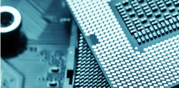
Substrate packaging is a critical process in semiconductor and electronic product manufacturing, involving the mounting and interconnection of electronic components on a base material called a substrate. This technology provides mechanical support, electrical connections, and thermal management for integrated circuits (ICs) and other electronic devices. Substrates can be made from various materials, including silicon, ceramics, and organic compounds, each offering unique properties to suit different applications.
Definition and Overview
Substrate packaging bridges the gap between the delicate semiconductor die and the more robust external environment. It ensures that electronic components are securely attached, electrically connected, and thermally managed. This process is integral to creating high-performance, reliable, and miniaturized electronic products.
Importance in Semiconductors and Electronic Products
Substrate packaging plays a vital role in the functionality and efficiency of semiconductor devices and electronic products. It directly impacts the device’s performance, durability, and size. With the ongoing trend towards miniaturization and increased functionality in electronics, advanced substrate packaging technologies are essential for meeting the demands of modern applications in consumer electronics, telecommunications, automotive systems, and more.
Background of Substrate Packaging Technology
Definition of Substrate in Technology
In technology, a substrate is a foundational layer upon which other materials are deposited or onto which electronic components are assembled. This base layer can be composed of various materials, such as silicon, glass, ceramics, or organic compounds, depending on the application. The substrate serves as the supporting structure for the intricate components that constitute electronic devices and systems.
Role of Substrate in Various Technology Fields
Substrates play a pivotal role across multiple technology fields. In electronics, they provide the base for mounting and interconnecting semiconductor devices, such as integrated circuits (ICs), LEDs, and sensors. In the field of photovoltaics, substrates support thin-film solar cells. In biotechnology, substrates are used as surfaces for cell cultures and biosensors. Across these domains, substrates facilitate the integration and functioning of complex assemblies, ensuring structural stability and optimal performance.
Relationship to Substrate in Chip Design
In chip design, the substrate is fundamental to the overall architecture of an IC. It serves as the physical platform upon which semiconductor devices are built. Silicon is the most common material used for substrates in chip design due to its excellent electrical properties and availability. The substrate not only supports the devices mechanically but also plays a critical role in heat dissipation and electrical insulation, which are vital for the reliable operation of high-density electronic circuits.
Difference Between Substrate and Package
Definitions and Functional Differences
While substrates and packages are both integral to semiconductor technology, they serve distinct purposes. A substrate is the base material on which semiconductor devices are fabricated or mounted. It provides mechanical support, electrical connectivity, and thermal management. On the other hand, a package is the final enclosure that encases the semiconductor devices, protecting them from physical damage and environmental contaminants. The package also includes external connections that allow the semiconductor devices to interface with other system components.
Applications in Semiconductor Manufacturing
In semiconductor manufacturing, substrates are used in the initial stages of device fabrication. For instance, in the production of ICs, a silicon wafer acts as the substrate on which transistors and other circuit elements are constructed. Once the semiconductor devices are fabricated on the substrate, they are then packaged to form the final product. The package provides additional features such as improved thermal management, enhanced electrical performance, and physical protection, which are essential for the durability and functionality of the semiconductor devices in real-world applications.
Understanding the differences and roles of substrates and packages is crucial for advancing semiconductor technology and developing high-performance electronic devices. The ongoing innovations in substrate materials and packaging techniques continue to drive the miniaturization, efficiency, and reliability of modern electronics.
Technological Development of Substrate Packaging
Transition from Traditional PCBs to Modern Package Substrates
The evolution of substrate packaging technology has been marked by significant transitions, starting from traditional printed circuit boards (PCBs) to advanced package substrates. Traditional PCBs, primarily used for mounting and interconnecting electronic components, were limited in their capability to support high-density and high-performance applications. With the increasing complexity and miniaturization of electronic devices, the need for more advanced substrate technologies became evident.
Modern package substrates emerged to address these limitations, offering enhanced electrical performance, improved thermal management, and higher mechanical stability. These substrates integrate multiple layers of interconnects and advanced materials, enabling the construction of more compact and efficient electronic assemblies. The shift from single-layer PCBs to multi-layer substrates marked a significant milestone, allowing for greater component density and more complex circuit designs.
Key Technological Advancements and Milestones
Several key technological advancements have driven the development of substrate packaging technology:
- Multi-Layer Substrates: The introduction of multi-layer substrates allowed for increased circuit density and complexity, enabling the integration of more functionalities within a smaller footprint.
- High-Density Interconnect (HDI) Technology: HDI technology revolutionized substrate packaging by enabling finer lines and spaces, microvias, and buried vias. This technology significantly enhanced the electrical performance and miniaturization of electronic devices.
- Advanced Materials: The development and use of advanced materials such as low-loss dielectrics, high thermal conductivity substrates, and flexible substrates have improved the performance and reliability of substrate packages.
- System-in-Package (SiP) Technology: SiP technology allows for the integration of multiple ICs and passive components within a single package, reducing the overall size and improving the performance of electronic systems.
- 3D Packaging: The advent of 3D packaging techniques, including through-silicon vias (TSVs) and wafer-level packaging (WLP), has further enhanced the integration and performance of electronic devices by enabling vertical stacking of components.
Latest Trends in Substrate Packaging Technology
The field of substrate packaging technology is continuously evolving, driven by the demand for more powerful, efficient, and compact electronic devices. Some of the latest trends include:
- Miniaturization and Higher Integration: As devices become smaller, there is a growing need for substrates that support higher component density and integration. Technologies such as HDI, SiP, and 3D packaging are at the forefront of this trend.
- Advanced Thermal Management: With increasing power densities, effective thermal management has become critical. New substrate materials with high thermal conductivity, such as ceramic-based substrates and metal-core PCBs, are being developed to dissipate heat more efficiently.
- Flexible and Stretchable Substrates: Flexible and stretchable substrates are gaining traction in applications such as wearable electronics and flexible displays. These substrates allow for new form factors and innovative device designs.
- Environmentally Friendly Materials: There is a growing emphasis on using environmentally friendly and sustainable materials in substrate manufacturing. This includes the development of biodegradable substrates and the reduction of hazardous substances in electronic products.
Application of New Materials and Processes
The continuous improvement of substrate packaging technology relies heavily on the application of new materials and processes. Some of the notable advancements include:
- Low-Loss Dielectric Materials: These materials reduce signal loss and improve the overall electrical performance of substrates, making them ideal for high-frequency applications such as 5G and high-speed data communications.
- High-Thermal-Conductivity Materials: Advanced materials with high thermal conductivity are being used to enhance heat dissipation in high-power applications, ensuring the reliability and longevity of electronic devices.
- Additive Manufacturing: Additive manufacturing techniques, such as 3D printing, are being explored for substrate fabrication. These processes offer greater design flexibility, reduced material waste, and the potential for on-demand production.
- Nano-Materials: The use of nano-materials, including graphene and carbon nanotubes, is being investigated to improve the electrical, thermal, and mechanical properties of substrates. These materials offer the potential for significant performance enhancements in next-generation electronic devices.
By embracing these trends and innovations, the substrate packaging industry continues to push the boundaries of what is possible, enabling the creation of more advanced, efficient, and reliable electronic systems.
Key Materials and Processes in Substrate Packaging
Package Substrate Materials
Common Types of Substrate Materials and Their Properties
- Silicon (Si):
- Properties: High thermal conductivity, excellent electrical properties, and compatibility with standard semiconductor processes.
- Applications: Widely used in integrated circuits (ICs) and microelectromechanical systems (MEMS).
- Pros: High purity, well-established processing techniques, and excellent thermal management.
- Cons: Brittle, high cost, and limited flexibility.
- Ceramics (Alumina, Aluminum Nitride, Silicon Carbide):
- Properties: High thermal conductivity, good electrical insulation, and excellent mechanical strength.
- Applications: Power electronics, high-frequency applications, and LED packaging.
- Pros: Superior thermal management, high durability, and stability in harsh environments.
- Cons: Expensive, challenging to process, and brittle.
- Organic Substrates (FR4, BT Resin, Polyimide):
- Properties: Good electrical insulation, flexibility, and lower cost compared to ceramic and silicon substrates.
- Applications: Printed circuit boards (PCBs), flexible electronics, and consumer electronics.
- Pros: Cost-effective, flexible, and easy to process.
- Cons: Lower thermal conductivity, lower mechanical strength, and potential for moisture absorption.
- Metal-Core PCBs (MCPCBs):
- Properties: Incorporate a metal core (typically aluminum or copper) for improved thermal management.
- Applications: High-power LED lighting, power supplies, and automotive electronics.
- Pros: Excellent heat dissipation, improved mechanical strength, and reliability.
- Cons: Higher cost, complex manufacturing processes, and weight considerations.
- Flexible Substrates (Kapton, PET):
- Properties: Highly flexible, lightweight, and suitable for dynamic applications.
- Applications: Wearable electronics, flexible displays, and medical devices.
- Pros: Flexibility, lightweight, and adaptable to various form factors.
- Cons: Lower thermal and mechanical strength, and potential issues with long-term reliability.
Applications and Pros and Cons of Different Materials
Each substrate material has its specific applications, driven by its inherent properties:
- Silicon: Ideal for high-performance ICs and MEMS due to its excellent electrical and thermal properties, but its brittleness and high cost limit its use in some applications.
- Ceramics: Preferred for high-power and high-frequency applications because of their superior thermal management, though their brittleness and processing difficulty are drawbacks.
- Organic Substrates: Common in consumer electronics and PCBs for their cost-effectiveness and ease of processing, but they suffer from lower thermal and mechanical performance.
- Metal-Core PCBs: Used where effective heat dissipation is crucial, such as in LED and power electronics, despite their higher cost and complex manufacturing.
- Flexible Substrates: Essential for applications requiring flexibility and lightweight, though they need to overcome challenges in thermal and mechanical performance.
Manufacturing Processes
Major Steps in Substrate Manufacturing
- Material Preparation:
- Silicon Substrates: Slicing silicon wafers from ingots, followed by polishing and cleaning.
- Ceramic Substrates: Forming ceramic sheets through processes like tape casting, followed by sintering.
- Organic Substrates: Laminating layers of resin and fiber glass, curing, and pressing.
- Patterning:
- Photolithography: Applying photoresist, exposing patterns using UV light, and developing the image.
- Etching: Removing unwanted material through chemical or plasma etching to create circuit patterns.
- Layer Stacking:
- Multi-Layer Substrates: Aligning and bonding multiple patterned layers, often using lamination and pressing techniques.
- Drilling and Via Formation:
- Mechanical Drilling: Creating holes for vias and interconnects.
- Laser Drilling: Precision drilling for microvias in HDI substrates.
- Metallization:
- Electroplating and Sputtering: Depositing conductive materials (copper, gold) onto the substrate for interconnections.
- Inspection and Testing:
- Optical Inspection: Checking for defects and alignment issues.
- Electrical Testing: Ensuring continuity and performance of the interconnections.
Key Technical Challenges and Solutions
- Thermal Management:
- Challenge: Efficiently dissipating heat in high-power applications.
- Solution: Using high-thermal-conductivity materials (ceramics, metal-core PCBs) and advanced thermal interface materials.
- Miniaturization and High-Density Interconnects:
- Challenge: Achieving higher component density and finer line/space widths.
- Solution: Adopting HDI technology, microvia drilling, and advanced photolithography techniques.
- Material Compatibility and Integration:
- Challenge: Ensuring compatibility between different materials and layers.
- Solution: Careful selection of materials with matching thermal expansion coefficients and robust bonding techniques.
- Mechanical Reliability:
- Challenge: Maintaining mechanical integrity under stress and environmental conditions.
- Solution: Utilizing flexible and robust materials, and incorporating design features that enhance mechanical stability.
By addressing these challenges with innovative solutions, substrate manufacturing continues to advance, enabling the development of more efficient, reliable, and high-performance electronic devices.
Career Opportunities in Substrate Packaging Technology Development
Overview of Substrate Packaging Technology Development Jobs
The field of substrate packaging technology offers a wide range of career opportunities for professionals with various backgrounds in engineering, materials science, and manufacturing. As the demand for advanced electronic devices continues to grow, so does the need for skilled individuals who can contribute to the development and optimization of substrate packaging technologies.
Typical Job Descriptions and Requirements
- Substrate Packaging Engineer:
- Job Description: Responsible for designing, developing, and testing substrate packages for semiconductor devices. This role involves collaborating with cross-functional teams to ensure that the substrate designs meet performance, reliability, and cost targets.
- Requirements:
- Bachelor’s or Master’s degree in Electrical Engineering, Materials Science, or a related field.
- Experience with substrate design tools (e.g., CAD software).
- Knowledge of substrate materials, manufacturing processes, and industry standards.
- Strong problem-solving skills and attention to detail.
- Materials Scientist – Substrate Development:
- Job Description: Focuses on researching and developing new materials for substrate packaging. This includes evaluating material properties, conducting experiments, and collaborating with suppliers to identify and qualify new materials.
- Requirements:
- Ph.D. or Master’s degree in Materials Science, Chemistry, or a related field.
- Hands-on experience with material characterization techniques (e.g., SEM, XRD).
- Strong analytical skills and ability to interpret experimental data.
- Excellent communication and teamwork skills.
- Process Development Engineer:
- Job Description: Develops and optimizes manufacturing processes for substrate packaging. This role involves working closely with production teams to implement new processes, troubleshoot issues, and ensure high-quality production.
- Requirements:
- Bachelor’s or Master’s degree in Chemical Engineering, Mechanical Engineering, or a related field.
- Experience with process development and optimization in a manufacturing environment.
- Knowledge of statistical process control (SPC) and Six Sigma methodologies.
- Strong project management and problem-solving abilities.
- Quality Assurance Engineer:
- Job Description: Ensures the quality and reliability of substrate packages through rigorous testing and inspection. This role involves developing quality control plans, conducting failure analysis, and implementing corrective actions.
- Requirements:
- Bachelor’s degree in Engineering, Materials Science, or a related field.
- Experience with quality assurance and testing in the semiconductor industry.
- Familiarity with industry standards (e.g., IPC, JEDEC).
- Strong analytical and documentation skills.
- Product Manager – Substrate Packaging:
- Job Description: Manages the development and commercialization of new substrate packaging products. This role involves market research, product planning, and coordinating with engineering and sales teams to ensure successful product launches.
- Requirements:
- Bachelor’s degree in Engineering, Business, or a related field.
- Experience in product management or a related role in the semiconductor industry.
- Strong understanding of market trends and customer needs.
- Excellent leadership and communication skills.
Active Companies in the Field
Several companies are leading the way in substrate packaging technology, each with its own strengths and market positions:
- Advanced Semiconductor Engineering (ASE) Group:
- Technological Strengths: ASE is one of the largest providers of semiconductor packaging and testing services. The company is known for its innovative packaging solutions, including system-in-package (SiP) and wafer-level packaging (WLP) technologies.
- Market Position: ASE has a strong global presence and is a key player in the semiconductor manufacturing supply chain.
- Taiwan Semiconductor Manufacturing Company (TSMC):
- Technological Strengths: TSMC is renowned for its advanced semiconductor fabrication technologies. The company also invests heavily in advanced packaging solutions, such as 3D ICs and chip-on-wafer-on-substrate (CoWoS) technology.
- Market Position: TSMC is the world’s largest dedicated semiconductor foundry, commanding a significant share of the global market.
- Amkor Technology:
- Technological Strengths: Amkor is a leading provider of outsourced semiconductor packaging and test services. The company offers a broad range of packaging solutions, including flip chip, 3D packaging, and MEMS packaging.
- Market Position: Amkor is a major player in the semiconductor packaging industry, with a strong focus on innovation and customer service.
- Samsung Electronics:
- Technological Strengths: Samsung is a global leader in semiconductor technology, known for its cutting-edge memory, logic, and foundry solutions. The company’s advanced packaging technologies include fan-out wafer-level packaging (FOWLP) and integrated fan-out (InFO) technology.
- Market Position: Samsung is a top-tier semiconductor manufacturer with a robust market position and a strong focus on research and development.
- Intel Corporation:
- Technological Strengths: Intel is a leader in semiconductor innovation, with a strong emphasis on advanced packaging technologies. The company has pioneered several packaging solutions, including Embedded Multi-Die Interconnect Bridge (EMIB) and Foveros 3D packaging.
- Market Position: Intel is a dominant player in the semiconductor industry, known for its high-performance processors and innovative packaging solutions.
By working at these companies, professionals in substrate packaging technology development can contribute to cutting-edge advancements in the semiconductor industry, shaping the future of electronic devices and systems.
Future of Substrate Packaging Technology
Potential Technological Breakthroughs and Trends in the Coming Years
- Advanced Materials:
- Graphene and Nanomaterials: The use of graphene and other nanomaterials in substrate packaging is anticipated to revolutionize the field. These materials offer superior electrical, thermal, and mechanical properties, enabling the development of ultra-high-performance substrates.
- Flexible and Biodegradable Substrates: Research into flexible and biodegradable substrates is gaining traction. These materials could lead to innovative applications in wearable electronics and environmentally friendly devices.
- 3D Packaging and Integration:
- Through-Silicon Vias (TSVs): The adoption of TSVs for 3D IC packaging will continue to grow, allowing for increased performance and reduced form factor by vertically stacking chips.
- Wafer-Level Packaging (WLP): WLP technology will advance, offering improved performance and reduced cost by integrating multiple dies at the wafer level.
- Heterogeneous Integration:
- System-in-Package (SiP): SiP technology, which integrates multiple heterogeneous components (e.g., logic, memory, sensors) into a single package, will become more prevalent. This integration will enhance device performance, functionality, and miniaturization.
- Chiplet Architecture: The use of chiplet architecture, where smaller chips (chiplets) are interconnected on a common substrate, will gain momentum. This approach offers design flexibility, scalability, and cost efficiency.
- Thermal Management Innovations:
- Embedded Cooling Solutions: New cooling technologies, such as embedded microfluidic channels within substrates, will improve heat dissipation and enable higher power densities.
- Advanced Thermal Interface Materials (TIMs): Development of superior TIMs with high thermal conductivity will enhance the thermal performance of substrates.
Emerging Applications and Market Opportunities
- 5G and Beyond:
- The rollout of 5G networks and the development of 6G will drive demand for advanced substrate packaging solutions capable of supporting high-frequency and high-speed applications.
- Internet of Things (IoT):
- The proliferation of IoT devices will require cost-effective, miniaturized, and highly integrated substrate solutions, creating significant market opportunities.
- Wearable and Flexible Electronics:
- The growing market for wearable devices will spur innovation in flexible and stretchable substrates, enabling new form factors and applications.
- Automotive Electronics:
- Advances in autonomous driving, electric vehicles, and connected car technologies will increase the need for robust, high-performance substrate packaging solutions capable of withstanding harsh automotive environments.
- Healthcare and Biomedical Devices:
- The development of advanced biomedical devices and implants will drive demand for biocompatible and flexible substrates, supporting innovations in health monitoring and diagnostics.
Substrate packaging technology is at the heart of modern electronic device manufacturing, enabling the integration of complex functionalities within compact and efficient packages. As technology advances, substrate packaging continues to evolve, driven by the need for higher performance, greater miniaturization, and improved thermal management.
Importance and Impact of Substrate Packaging Technology
The importance of substrate packaging technology cannot be overstated. It is a critical enabler of high-performance computing, telecommunications, consumer electronics, and emerging applications such as IoT, wearable electronics, and automotive systems. Advances in substrate packaging directly impact the efficiency, reliability, and functionality of electronic devices, making it a cornerstone of technological innovation.
Expectations and Prospects for Future Development
The future of substrate packaging technology is bright, with numerous potential breakthroughs on the horizon. The continued development of advanced materials, 3D packaging techniques, and heterogeneous integration will drive the industry forward. Emerging applications in 5G, IoT, automotive electronics, and healthcare will create new market opportunities and demand for innovative substrate solutions.
Substrate packaging technology is poised to play an increasingly vital role in the advancement of electronics, enabling the next generation of high-performance, reliable, and miniaturized devices. As research and development efforts continue, we can expect to see significant innovations that will shape the future of technology and open up new possibilities for electronic applications across various industries.
FAQs About substrate packaging technology development
Substrate packaging refers to the process of mounting and interconnecting electronic components onto a base material (substrate). It provides mechanical support, electrical connections, and thermal management for integrated circuits (ICs) and other electronic devices.
In technology, a substrate is a foundational material onto which other materials are deposited or electronic components are assembled. It serves as a base or support for building complex electronic circuits and devices.
A substrate is the underlying material (such as silicon, ceramic, or organic compound) on which electronic components are mounted and interconnected. In contrast, a package is the outer enclosure that houses the semiconductor device, providing protection and external connections.
In chip design, a substrate refers to the base material (usually silicon) on which semiconductor devices like transistors and diodes are fabricated. The substrate provides structural support and electrical connections for the integrated circuit components.

