
Choosing the Right Substrate Material for Semiconductors
In the intricate world of semiconductor manufacturing, substrate materials play a pivotal role in ensuring the reliability, performance, and longevity of electronic devices. These materials form the foundation upon which semiconductor components are built, providing structural support, electrical connectivity, and thermal management. Substrates are not merely passive carriers; they are integral to the functionality and miniaturization of modern semiconductor devices, facilitating the integration of complex circuits and enabling the compact designs demanded by today’s technology. Understanding the diverse properties and applications of substrate materials is crucial for optimizing semiconductor packaging processes, enhancing device performance, and meeting the evolving demands of industries ranging from consumer electronics to aerospace. This article explores the key considerations and advancements in substrate materials essential for the next generation of semiconductor technologies.
What is a Substrate in Semiconductor Packaging?
In semiconductor manufacturing, a substrate refers to a foundational material on which semiconductor components are fabricated and interconnected to form integrated circuits (ICs). The substrate serves several critical functions that are indispensable to the functionality and performance of semiconductor devices.
Definition of substrate in the context of semiconductor manufacturing
A substrate typically consists of a thin, flat base material, often made of silicon, ceramic, or specialized polymers, upon which semiconductor devices are mounted and interconnected. It provides a stable platform for attaching semiconductor chips and other components during the assembly process.
Role of substrates in providing structural support and electrical connections
- Structural Support: Substrates offer mechanical strength and rigidity, ensuring the integrity and durability of semiconductor devices. They help to withstand thermal and mechanical stresses encountered during manufacturing, assembly, and operation.
- Electrical Connections: Substrates facilitate electrical connections between semiconductor components and external circuitry. They often feature intricate patterns of conductive traces, known as interconnects, which link the semiconductor chips to external pins or contacts. These interconnects enable the transmission of signals, power, and data throughout the device.
In essence, substrates serve as a crucial interface between semiconductor components and the broader electronic system, enabling efficient operation and integration into various applications across industries. Understanding their role and selecting appropriate substrate materials are fundamental to optimizing semiconductor packaging processes and enhancing overall device performance.
Common Substrate Materials for Semiconductors
Silicon (Si) Substrates
Properties and Suitability for Semiconductor Manufacturing:
Silicon (Si) is the most widely used substrate material in semiconductor manufacturing due to its abundance, excellent semiconductor properties, and well-established fabrication processes. Silicon substrates are typically single-crystal structures with high purity, allowing for precise control over electronic properties such as carrier mobility and conductivity. These properties make silicon ideal for producing integrated circuits (ICs) that require high performance and reliability.
Advantages:
- Abundance and Cost-effectiveness: Silicon is abundant in nature, making it cost-effective for large-scale semiconductor production.
- Compatibility: Silicon substrates integrate well with existing semiconductor fabrication technologies, enabling high-yield manufacturing processes.
- Versatility: Silicon substrates support a wide range of semiconductor device types, from microprocessors to memory chips.
Limitations:
- Thermal Conductivity: Silicon has moderate thermal conductivity compared to other materials, which can be a limitation in high-power applications.
- Mechanical Strength: Silicon substrates can be brittle, requiring careful handling during manufacturing and assembly processes.
Gallium Arsenide (GaAs) Substrates
Applications and Characteristics in Semiconductor Devices:
Gallium Arsenide (GaAs) substrates are primarily used in high-frequency and optoelectronic applications due to their superior electron mobility and direct bandgap properties. GaAs substrates are especially suited for devices such as microwave amplifiers, solar cells, and high-speed digital circuits where high-frequency operation and efficiency are critical.
Comparison with Silicon Substrates:
- Performance: GaAs substrates offer higher electron mobility than silicon, leading to faster transistor switching speeds and better performance in high-frequency applications.
- Optoelectronics: GaAs substrates are essential for optoelectronic devices like LEDs and photovoltaic cells due to their direct bandgap, which enables efficient light emission and absorption.
- Cost: GaAs substrates are generally more expensive than silicon due to lower availability and more specialized manufacturing processes.
Gallium Nitride (GaN) Substrates
Emerging Trends and Applications:
Gallium Nitride (GaN) substrates have gained prominence in recent years for their applications in high-power and high-frequency devices, including power electronics, RF amplifiers, and LEDs. GaN substrates offer excellent electrical properties such as high electron mobility and a wide bandgap, enabling efficient operation at high voltages and frequencies.
Key Properties for High-Power Devices:
- High Breakdown Voltage: GaN substrates can withstand higher voltages than silicon, making them suitable for power electronics applications.
- Efficiency: GaN substrates exhibit low on-resistance and high switching speeds, leading to improved energy efficiency and reduced heat dissipation.
- Miniaturization: GaN substrates enable the development of compact and lightweight power electronic devices due to their high power density and thermal management capabilities.
The choice of substrate material significantly influences the performance, efficiency, and application range of semiconductor devices. Each material offers unique advantages and considerations, shaping their suitability for various semiconductor manufacturing needs and emerging technological trends.
Semiconductor Packaging Materials
Semiconductor packaging materials play a crucial role in protecting delicate semiconductor devices while enhancing their performance and reliability. Here’s an in-depth look at the materials commonly used in semiconductor packaging:
Overview of Materials Used in Semiconductor Packaging
- Ceramics:
- Alumina (Al₂O₃) and Aluminum Nitride (AlN): These ceramics are widely used for their excellent thermal conductivity and electrical insulation properties. They are commonly employed in high-power semiconductor devices where heat dissipation is critical.
- Metals:
- Copper (Cu) and Aluminum (Al): Metals are used for their high electrical conductivity, which is essential for efficient electrical connections within semiconductor packages. Copper is preferred for its superior conductivity, while aluminum is used in applications where cost and weight are considerations.
- Plastics and Polymers:
- Epoxy Molding Compounds (EMCs): EMCs are thermosetting plastics used for encapsulating semiconductor chips. They provide mechanical protection, moisture resistance, and a level of electrical insulation. EMCs are cost-effective and widely used in consumer electronics.
- Adhesives and Sealants:
- Silicone and Epoxy Adhesives: These materials are used for bonding semiconductor components to substrates and for sealing the package to protect against environmental factors such as moisture and dust.
- Dielectric Materials:
- Polyimides, Parylene, and Silicon Nitride: These materials are used as thin films or coatings to provide electrical insulation, passivation, and protection against corrosion and mechanical stress.
Importance of Materials in Protecting Semiconductor Devices and Improving Performance
- Environmental Protection: Semiconductor packaging materials shield devices from external contaminants such as moisture, dust, and chemicals, which can degrade performance and reliability over time.
- Mechanical Support: Packaging materials provide structural integrity, protecting semiconductor chips from physical damage during handling, assembly, and operation.
- Thermal Management: Materials with high thermal conductivity, such as ceramics and certain metals, help dissipate heat generated by semiconductor devices. Effective thermal management is crucial for maintaining device performance and preventing thermal-induced failures.
- Electrical Performance: Proper selection and design of packaging materials ensure minimal electrical losses, signal integrity, and reliable electrical connections between semiconductor components and external circuitry.
In essence, semiconductor packaging materials are critical for safeguarding devices, enhancing their operational capabilities, and ensuring long-term reliability in a wide range of applications from consumer electronics to automotive and industrial sectors. Advances in packaging materials continue to drive innovations in semiconductor technology, enabling smaller, faster, and more efficient electronic devices.
Package Substrate vs. PCB
Definition and Differences between Package Substrate and Printed Circuit Board (PCB)
Package Substrate
- Definition: A package substrate, also known as a chip carrier or substrate, is a specialized substrate material used specifically for mounting and interconnecting semiconductor chips (ICs) within a semiconductor package. It typically includes conductive traces, vias, and bonding pads designed to facilitate electrical connections between the semiconductor device and external circuitry.
- Material: Package substrates are often made from materials like ceramics (e.g., alumina, aluminum nitride), organic laminates (e.g., FR-4), or specialized polymers (e.g., BT resin) tailored to meet the electrical, thermal, and mechanical requirements of the semiconductor package.
Printed Circuit Board (PCB)
- Definition: A PCB is a generic term referring to a rigid or flexible board made of insulating material (e.g., fiberglass-reinforced epoxy resin) with conductive pathways (traces) etched or printed onto its surface. PCBs are used to mechanically support and electrically connect electronic components using soldered connections.
- Role: PCBs serve as the backbone of electronic systems, providing a platform for mounting and interconnecting various electronic components such as resistors, capacitors, and integrated circuits (ICs). They are essential for routing signals and power between components and external interfaces.
Role of Each in Semiconductor Device Assembly and Functionality
Package Substrate
- Assembly: Package substrates are specifically designed to house and interconnect semiconductor chips, providing a robust interface that facilitates electrical connections, thermal dissipation, and mechanical stability. They often include advanced features such as microvias and flip-chip bonding for high-density interconnects and efficient heat transfer.
- Functionality: Package substrates play a crucial role in ensuring the electrical performance and reliability of semiconductor devices. They enable compact and efficient integration of semiconductor chips into packages, supporting high-speed data transmission, power delivery, and signal integrity.
Printed Circuit Board (PCB)
- Assembly: PCBs serve as the primary platform for assembling and interconnecting a wide range of electronic components beyond semiconductor chips, including passive components and connectors. They facilitate the soldering of components onto the board and the routing of electrical connections between them.
- Functionality: PCBs provide the structural and electrical framework for electronic devices, enabling complex circuits to be realized in a compact and organized manner. They support diverse functionalities, from simple signal routing in consumer electronics to complex computing tasks in advanced electronic systems.
While both package substrates and PCBs play critical roles in semiconductor device assembly and functionality, they serve distinct purposes. Package substrates focus on optimizing the integration and performance of semiconductor chips within a package, while PCBs provide the broader infrastructure for assembling and interconnecting various electronic components in electronic systems. Together, they enable the design and production of sophisticated and reliable electronic devices across industries.
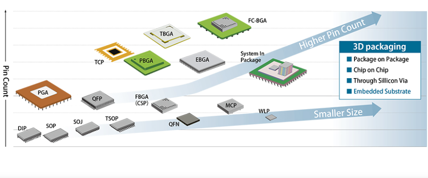
Semiconductor Packaging Types
Flip Chip Technology
Description and Advantages in Packaging: Flip chip technology is a method of semiconductor packaging where the active side of the semiconductor die (chip) faces downward and is directly connected to the package substrate or PCB using solder bumps. This contrasts with traditional wire bonding, where connections are made to the chip’s perimeter.
Advantages:
- Size and Performance: Flip chip technology enables smaller package sizes and shorter interconnect lengths, leading to improved electrical performance, higher speed operation, and reduced signal delays.
- Heat Dissipation: Direct thermal and electrical connections between the chip and substrate or PCB facilitate efficient heat dissipation, enhancing device reliability and longevity.
- Signal Integrity: Shorter interconnect lengths reduce parasitic capacitance and inductance, improving signal integrity and reducing electromagnetic interference (EMI).
Substrate Materials Used in Flip Chip Technology:
- Organic Substrates (e.g., BT Resin): Cost-effective and widely used for consumer electronics applications.
- Ceramic Substrates (e.g., Alumina, Aluminum Nitride): Provide superior thermal conductivity and mechanical strength, suitable for high-power and high-frequency applications.
- Flexible Substrates (e.g., Polyimide): Used in applications requiring flexibility or conformal packaging.
Wire Bonding
Basics of Wire Bonding in Semiconductor Packaging: Wire bonding is a technique used to connect semiconductor chips to the package substrate or PCB using fine wires (typically gold or aluminum) that are thermally and mechanically bonded to bonding pads on the chip and substrate/PCB.
Suitable Substrate Materials for Wire Bonding:
- Gold and Aluminum Bonding Pads: Commonly used on silicon and other semiconductor materials.
- Aluminum and Copper Substrates: Provide good thermal and electrical properties for wire bonding applications.
- Ceramic Substrates: Offer high mechanical strength and thermal conductivity, suitable for wire bonding in high-power applications.
Comparison with Flip Chip Technology:
- Performance: Wire bonding is generally less expensive and easier to implement for low-pin-count devices but may have limitations in high-frequency and high-power applications compared to flip chip technology.
- Applications: Wire bonding remains prevalent in a wide range of semiconductor devices, including microcontrollers, memory chips, and discrete components, where cost-effectiveness and reliability are critical.
The choice between flip chip technology and wire bonding depends on the specific requirements of the semiconductor device, including performance goals, cost considerations, and application needs. Both technologies continue to evolve to meet the demands of advancing semiconductor technologies across various industries.
Semiconductor Packaging Process
The semiconductor packaging process involves several key steps to encapsulate and protect semiconductor chips (ICs) while providing electrical connections to external circuitry. Here’s a detailed overview:
Steps Involved in Semiconductor Packaging
- Die Preparation:
- Singulation: Individual semiconductor chips are separated (singulated) from the wafer using dicing saws or laser cutting.
- Backside Grinding (optional): Thinning the semiconductor die to reduce thickness and improve thermal management.
- Die Attach:
- The semiconductor die is attached (bonded) to the package substrate or PCB using adhesive materials or soldering techniques. This step ensures mechanical stability and thermal conductivity between the die and substrate.
- Wire Bonding or Flip Chip Bonding:
- Wire Bonding: Fine wires (gold or aluminum) are bonded between the semiconductor die and the package substrate or PCB to establish electrical connections.
- Flip Chip Bonding: Solder bumps or balls on the semiconductor die are directly bonded to corresponding pads on the package substrate or PCB, typically using reflow soldering techniques.
- Encapsulation:
- The semiconductor die and wire bonds (if applicable) are encapsulated with epoxy molding compounds (EMCs) or other encapsulation materials. This step protects the die from mechanical damage, moisture, and contaminants.
- Testing and Inspection:
- Comprehensive electrical testing is conducted to ensure the functionality and reliability of the packaged semiconductor devices. Various tests, including functional testing and reliability testing (such as temperature cycling and humidity testing), may be performed.
- Trim and Form:
- The packaged semiconductor devices are trimmed and formed to meet specific mechanical and dimensional requirements for integration into final products or electronic assemblies.
- Marking and Packaging:
- Devices are marked with identification codes, logos, and other information. They are then packaged in protective materials (e.g., trays, tubes, reels) suitable for shipment and handling.
Importance of Substrate Materials at Each Stage of the Packaging Process
- Die Attach: Substrate materials with appropriate thermal conductivity and mechanical strength are crucial for efficient heat dissipation and mechanical stability during die attachment.
- Wire Bonding or Flip Chip Bonding: The substrate must provide reliable electrical pathways and support for bonding techniques. Materials with good adhesion properties and appropriate thermal expansion coefficients help ensure robust interconnections.
- Encapsulation: Substrate materials influence the adhesion and compatibility of encapsulation materials. They also affect the thermal and mechanical properties of the final packaged device, impacting long-term reliability and performance.
- Testing and Inspection: Substrate materials can affect the electrical performance and reliability of the packaged devices during testing. Ensuring consistent substrate properties helps maintain uniform test results and device quality.
- Trim and Form: Substrate materials with good dimensional stability and mechanical integrity are essential for accurate trimming and forming processes, ensuring final device specifications are met.
Substrate materials play a critical role throughout the semiconductor packaging process, influencing the performance, reliability, and manufacturability of packaged semiconductor devices. Choosing suitable substrate materials tailored to specific packaging requirements is essential for achieving optimal device performance and ensuring successful integration into electronic systems.
FAQs About substrate material for semiconductors
In semiconductor packaging, a substrate refers to the material upon which semiconductor devices (chips) are mounted and interconnected. It provides structural support and electrical connections for the semiconductor components.
Silicon (Si) is the most common base material for semiconductors. It is widely used due to its abundance, excellent semiconductor properties, and compatibility with established fabrication processes.
In the context of silicon semiconductor manufacturing, the substrate refers to the silicon wafer itself. This wafer serves as the foundation upon which semiconductor devices are fabricated through processes like doping, etching, and deposition.
The substrate for semiconductor chips can vary depending on the specific application and technology. Common substrates include materials like silicon (for silicon-based chips), gallium arsenide (GaAs) for specialized applications, and various ceramic or organic materials used in package substrates for mounting and interconnecting the chips.

