
Understanding the Benefits of Substrate-Like PCB Technology
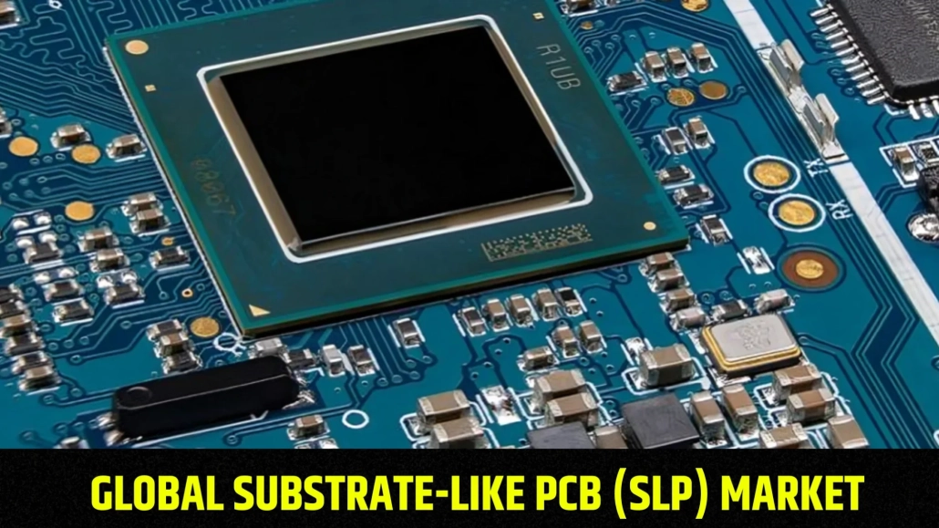
The substrate-like PCB (SLP) is an advanced type of printed circuit board that integrates IC substrate technology to achieve higher density and miniaturization. SLP features narrower trace widths and spaces compared to traditional PCBs, allowing for more components to be placed on a smaller area. This technological advancement is crucial in meeting the increasing demand for compact, high-performance electronic devices.
The importance of substrate-like PCB technology is particularly evident in modern consumer electronics such as smartphones and wearables, where space is limited, and performance is critical. SLP enables manufacturers to create thinner, more efficient devices with enhanced functionality and lower power consumption. As the demand for smaller, more powerful electronics continues to grow, SLP plays a vital role in enabling innovations in design and performance. Its ability to support high-density integration makes it a key technology in the development of next-generation electronic products.
Basics of Substrate-Like PCB
Origin and Evolution of Substrate-Like PCB
The origin of substrate-like PCB (SLP) technology can be traced back to the increasing need for higher-density and miniaturized electronics. Traditional printed circuit boards (PCBs), although effective for many years, faced limitations in accommodating the growing number of components required for advanced devices. As IC substrate technologies evolved, manufacturers began integrating their principles into PCB fabrication, leading to the development of SLP. This evolution allowed for narrower trace widths and higher interconnect densities, bridging the gap between standard PCBs and IC substrates. SLP technology emerged as an ideal solution to balance performance, size, and complexity in modern electronics.
What is Substrate-Like PCB Material?
The materials used in substrate-like PCB differ significantly from those in traditional PCBs. SLP materials are generally thinner, providing the necessary compactness while maintaining mechanical strength. These materials also offer superior conductivity, which is essential for supporting faster signal transmission, especially in high-performance devices. In terms of dielectric properties, SLP materials possess lower dielectric constants, reducing signal loss and enhancing signal efficiency. The use of these advanced materials allows substrate-like PCB to meet the stringent demands of space-constrained, high-density electronic devices. This material innovation plays a critical role in the continued advancement of consumer electronics and other high-tech applications.
Differences Between Substrate-Like PCB and Traditional PCB
Technical Differences Between Substrate-Like PCB and Regular PCB
Substrate-like PCB (SLP) technology introduces several key technical advancements over traditional PCBs, particularly in terms of design density, trace width, and manufacturing processes. SLP offers much higher design density by utilizing finer trace widths and spaces, typically ranging from 15 μm or less, whereas traditional PCBs generally operate with trace widths of 50 μm or more. This reduced trace width enables more components to be packed into a smaller area, allowing for the creation of compact and high-performance devices.
In terms of manufacturing, SLPs primarily rely on the modified semi-additive process (mSAP), which is more advanced than the subtractive etching process used in traditional PCBs. mSAP allows for precise patterning and thinner traces, which improves signal integrity and reduces signal loss. This process is essential for meeting the high-density interconnect (HDI) requirements in modern electronics. Additionally, SLP manufacturing often includes embedded components, enhancing overall system functionality, which is not common in traditional PCB fabrication.
Comparison Between Substrate-Like PCB and IC Substrates
While substrate-like PCB technology borrows heavily from IC substrate manufacturing techniques, there are important differences between the two. In terms of performance, IC substrates generally provide even finer feature sizes and higher interconnect densities than SLP, making them ideal for extremely miniaturized applications like semiconductor packaging. However, SLP strikes a balance between the ultra-high density of IC substrates and the lower cost of traditional PCBs, making it more suitable for consumer electronics like smartphones and wearables.
From a cost perspective, substrate-like PCB is more affordable than IC substrates, though it is typically more expensive than traditional PCBs due to the advanced materials and manufacturing processes involved. However, its price point makes it an attractive option for applications that demand higher performance but do not require the extreme specifications of IC substrates. In terms of application areas, SLP is widely used in devices requiring high integration and compact designs, while IC substrates are reserved for semiconductor-level interconnections in chips and high-end processors. This distinction positions SLP as a versatile solution for mass-market electronics.
SLP Manufacturing Process
Detailed Explanation of the mSAP Process
The modified semi-additive process (mSAP) is a core technology used in the manufacturing of substrate-like PCB (SLP). mSAP allows for the creation of ultra-fine circuit patterns, which are essential for achieving the higher design density found in SLPs. Unlike the traditional subtractive process used in regular PCBs, where copper is etched away from a larger sheet to form circuit patterns, mSAP begins with a thin layer of copper. This layer is selectively plated with additional copper where the traces will be, allowing for much narrower trace widths and spacing.
The mSAP process involves several precise steps: first, a thin seed layer of copper is applied to the substrate; next, a photoresist is used to define the trace patterns, followed by electroplating additional copper onto the exposed areas. After the photoresist is removed, the unwanted copper is etched away, leaving behind fine, accurate traces. This process results in trace widths as narrow as 15 µm, far finer than the 50 µm or greater typically found in traditional PCBs. The enhanced precision of mSAP contributes significantly to the miniaturization and performance improvements in substrate-like PCB manufacturing.
Embedded Component Packaging
One of the key innovations of substrate-like PCB (SLP) is its ability to integrate embedded components directly into the PCB structure. This packaging technique enhances functionality while reducing overall size, which is critical for modern electronics like smartphones, tablets, and wearable devices that require high-density integration in a compact form.
In SLP manufacturing, passive components such as resistors, capacitors, and inductors can be embedded within the inner layers of the board, freeing up valuable surface space for additional active components. These embedded components are interconnected through the fine traces produced via the mSAP process, enabling high-performance electronic designs. The inclusion of embedded components also enhances reliability by reducing the number of solder joints and external connections, which are common failure points in traditional PCB designs. This advanced packaging technique is one of the reasons why substrate-like PCB technology is a preferred choice for high-density and high-performance applications.
Applications of Substrate-Like PCB (SLP)
Applications in Smart Devices
Substrate-like PCB (SLP) technology plays a pivotal role in the design and performance of modern smart devices such as smartphones, tablets, and smartwatches. These devices demand compact designs with high-performance capabilities, and SLP enables manufacturers to meet these requirements through its advanced miniaturization and high-density integration. By using narrower trace widths and reduced component spacing, SLP allows more functions to be packed into smaller areas without compromising performance. This is especially important in smartphones, where space is limited, and components such as processors, memory, and communication modules must fit within increasingly thin and sleek designs.
For instance, SLP is often used in the mainboard of smartphones, where its enhanced signal integrity and reduced signal loss contribute to faster processing speeds and improved overall functionality. In smartwatches and tablets, SLP helps manufacturers integrate complex features like sensors, communication modules, and battery management systems into a confined space. This high-density integration not only enhances the functionality of smart devices but also contributes to longer battery life, thinner profiles, and better heat management—key factors that influence consumer satisfaction.
Automotive Electronics
As the automotive industry transitions towards electrification and smarter vehicle technologies, substrate-like PCB technology is becoming increasingly important. Electric vehicles (EVs), advanced driver-assistance systems (ADAS), and infotainment systems all require high-performance electronics that can handle complex functionalities while maintaining compactness. SLP’s ability to offer high-density circuit layouts is ideal for these applications, where space is often constrained, but performance and reliability are critical.
In automotive electronics, SLP is used in critical components such as control units, power management systems, and communication modules. The precise trace widths and enhanced signal integrity provided by the mSAP process ensure that these components can handle the high data processing requirements of modern vehicles. Additionally, the use of embedded component packaging in SLP helps reduce the size of control modules, which is essential for fitting these systems into increasingly compact spaces in vehicles.
Furthermore, the automotive industry’s shift towards EVs creates a demand for power-efficient, high-density PCBs that can manage electrical distribution, battery management, and onboard computer systems. SLP’s advanced materials and manufacturing techniques make it an ideal solution to meet these requirements, enabling more efficient power control and faster data transmission, both of which are essential in EV technology. As vehicles become more electrified and autonomous, substrate-like PCB technology will continue to play a key role in driving innovation in the automotive sector.
Key SLP Manufacturers
IC Substrate and SLP Manufacturers
Several leading manufacturers have established themselves as major players in the substrate-like PCB (SLP) and IC substrate market, utilizing their advanced technology to push the boundaries of miniaturization and high-density integration. One such company is AT&S, a global leader in high-end PCB and IC substrate production. AT&S has been at the forefront of integrating IC substrate technologies into SLP manufacturing, offering state-of-the-art products that meet the stringent demands of the electronics industry. With its focus on innovation, AT&S has positioned itself as a key supplier for the smartphone, automotive, and medical device sectors, providing advanced SLP solutions that support compact, high-performance designs. The company’s mSAP expertise and ability to embed components make it a top choice for customers requiring cutting-edge technologies.
Other prominent IC substrate and SLP manufacturers include Samsung Electro-Mechanics and Ibiden, both of which are recognized for their extensive expertise in miniaturization technologies. These companies leverage their experience in producing IC substrates to deliver high-quality substrate-like PCBs that meet the growing demand for next-generation electronic devices. Samsung’s integration of IC substrate technology into its SLP products has led to high-volume production of advanced PCBs used in smartphones and wearable devices. Similarly, Ibiden has developed a strong reputation for its precision in manufacturing high-density interconnects for consumer electronics and automotive applications.
SLP Manufacturers in China
China has emerged as a key hub for substrate-like PCB manufacturing, with several companies making significant contributions to the global market. Kinwong, a leading Chinese SLP manufacturer, has developed advanced capabilities in SLP production, offering high-density solutions to major electronics manufacturers around the world. Kinwong’s expertise in the mSAP process and its commitment to innovation have allowed it to become a critical supplier for high-end electronic products, including smartphones, tablets, and automotive electronics. The company is known for its efficient manufacturing processes and ability to scale production, which makes it a valuable player in the global SLP supply chain.
Another important manufacturer in China is Shenzhen Kinwong Electronics, which focuses on providing high-precision substrate-like PCBs for a wide range of applications. Shenzhen Kinwong Electronics has gained a reputation for producing reliable and high-performance SLPs, and its products are used in industries ranging from telecommunications to consumer electronics. Additionally, companies like Victory Giant Technology and Wus Printed Circuit are also making strides in the SLP market, further solidifying China’s position as a key contributor to the global substrate-like PCB industry.
China’s SLP manufacturers have not only contributed to lowering the cost of production through economies of scale but also have pushed forward innovation in materials and processes. Their ability to produce high-quality, cost-effective SLPs has enabled them to compete with global players, providing critical support for the rapid advancement of the consumer electronics and automotive sectors.
Future Trends in Substrate-Like PCB (SLP)
SLP Market Outlook
The substrate-like PCB (SLP) market is poised for significant growth as emerging technologies like 5G, the Internet of Things (IoT), and advanced consumer electronics continue to drive demand for high-performance, miniaturized devices. As 5G networks expand, devices will require enhanced data processing capabilities and increased bandwidth efficiency, which SLP’s high-density integration can deliver. The adoption of SLP in IoT applications is also expected to accelerate, given the need for compact, power-efficient components in interconnected devices such as smart home systems, industrial sensors, and wearable technology. These trends suggest a bright future for the SLP market, with ongoing investments in research and development to meet the demands of next-generation technologies.
Innovations in New Materials and Processes
The future of substrate-like PCB technology will also be shaped by advancements in materials and manufacturing processes. New materials with improved electrical conductivity, lower dielectric constants, and better thermal management properties are expected to enhance SLP performance, particularly in applications where power efficiency is critical. Additionally, innovations in mSAP and other manufacturing processes will enable even finer trace widths and higher component densities, allowing for more powerful and compact devices. These improvements will not only support the development of high-density, low-power electronics but also contribute to the ongoing miniaturization of devices in industries such as telecommunications, automotive electronics, and healthcare. The combination of material innovation and process refinement will be key to pushing the limits of SLP technology in the coming years.
Substrate-like PCB (SLP) material refers to a type of printed circuit board that integrates advanced IC substrate technology to achieve high-density interconnects and miniaturization. Unlike traditional PCBs, SLP materials are designed to support finer trace widths and tighter component spacing, enabling the creation of compact and high-performance electronic devices. SLP typically uses materials with improved electrical properties, such as lower dielectric constants and higher thermal conductivity, which contribute to better signal integrity and reduced power consumption. These materials are often combined with advanced manufacturing processes like the modified semi-additive process (mSAP) to achieve the precise, high-density patterns required for modern electronics.
PCB (Printed Circuit Board) and SLP (Substrate-Like PCB) differ primarily in their design density, manufacturing processes, and application areas:
Design Density: SLP offers much higher design density compared to traditional PCBs. It supports finer trace widths and spaces, which allows for more components to be integrated into a smaller area. This is essential for creating compact and high-performance devices.
Manufacturing Processes: SLP typically uses advanced manufacturing processes like the modified semi-additive process (mSAP) that enables high-precision circuit patterns and tighter component placement. Traditional PCBs often use subtractive etching processes, which have limitations in achieving the same level of density and precision.
Application Areas: SLP is often used in high-performance, space-constrained applications such as smartphones, tablets, and wearables. Traditional PCBs are used in a wider range of applications but may not meet the high-density requirements of modern electronic devices.
PCB Substrate and PCB Laminate refer to different components of a printed circuit board:
PCB Substrate: The substrate is the base material of a PCB that provides mechanical support and electrical insulation. It typically consists of a core material such as FR4 (a type of fiberglass-reinforced epoxy resin), which serves as the foundation upon which the conductive traces are built.
PCB Laminate: Laminate refers to the composite material that includes the substrate along with additional layers. It usually consists of a pre-impregnated resin (such as epoxy) that is bonded to the substrate and then cured. Laminate can include multiple layers of substrate material, copper foils, and other materials that are laminated together to form a complete PCB.
In essence, the substrate is a key component of the laminate, and the laminate includes the substrate along with additional layers that contribute to the overall functionality and structure of the PCB.
IC Substrate and PCB (Printed Circuit Board) differ in their primary functions, design requirements, and applications:
Function: IC substrates are specialized boards used to support and interconnect semiconductor chips (integrated circuits). They provide the necessary connections between the chip and the external circuitry. PCBs, on the other hand, are general-purpose boards used to physically support and electrically connect various electronic components in a wide range of electronic devices.
Design Requirements: IC substrates are designed to handle high-density interconnects and provide precise routing for signals. They often use advanced materials and manufacturing techniques to achieve fine-pitch connections and high-speed signal integrity. PCBs generally have larger trace widths and spacings, and they are less focused on high-density interconnects compared to IC substrates.
Applications: IC substrates are primarily used in semiconductor packaging for chips used in high-performance electronics, such as processors and memory devices. PCBs are used in a broad array of electronic products, including consumer electronics, industrial equipment, and automotive systems.

