
How to Choose the Right PLCC Chip Carrier
ABF substrate, short for Ajinomoto Build-up Film substrate, is a critical component in semiconductor packaging. It serves as a foundation for mounting and connecting semiconductor chips within electronic devices. ABF substrates consist of multiple layers of insulating material with embedded conductive traces, providing pathways for electrical signals to travel between components.
The significance of ABF substrate lies in its ability to support miniaturization and enhance the performance of electronic devices. Its high-density interconnection capability enables efficient signal transmission, contributing to faster processing speeds and improved overall functionality. As semiconductor technology continues to advance, the demand for ABF substrates grows, making them indispensable in the development of cutting-edge electronic products.
Understanding PLCC and BGA IC Packages
Definition of PLCC (Plastic Leaded Chip Carrier) package:
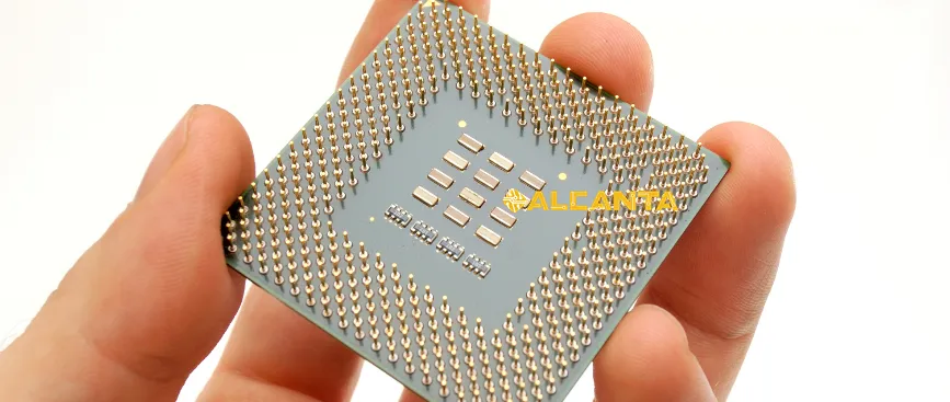
PLCC, or Plastic Leaded Chip Carrier, is a type of integrated circuit (IC) package characterized by its square or rectangular shape with leads (pins) extending from all four sides. The chip is mounted on a ceramic or plastic substrate within the package, and the leads are typically bent downwards to facilitate soldering onto the circuit board. PLCC packages offer good thermal performance and mechanical stability, making them suitable for a wide range of applications in the electronics industry.
Explanation of BGA (Ball Grid Array) IC package:
BGA, or Ball Grid Array, is another type of IC package commonly used in semiconductor packaging. Unlike PLCC, where leads extend from the sides of the package, BGA packages feature an array of solder balls on the bottom surface of the package. These solder balls serve as the interface between the package and the circuit board, providing electrical connections. BGA packages offer advantages such as higher pin count, smaller footprint, and improved electrical performance compared to traditional packages like PLCC.
Comparison between PLCC and BGA packages:
1. Form Factor: PLCC packages typically have leads extending from the sides, while BGA packages have solder balls on the bottom surface.
2. Pin Count: BGA packages generally offer higher pin counts compared to PLCC packages, allowing for more complex designs.
3. Size and Footprint: BGA packages tend to have a smaller footprint than PLCC packages, making them suitable for space-constrained applications.
4. Electrical Performance: BGA packages often exhibit better electrical performance due to shorter signal paths and reduced inductance.
5. Thermal Considerations: PLCC packages may offer better thermal performance compared to BGA packages due to the larger exposed surface area for heat dissipation.
6. Cost: BGA packages may be more expensive to manufacture and assemble than PLCC packages due to their complexity and higher pin density.
Overall, the choice between PLCC and BGA packages depends on factors such as the specific application requirements, cost considerations, and design constraints. Both package types have their advantages and are widely used in various electronic devices and systems.
Role of PLCC in Semiconductor Packaging
Overview of PLCC’s Function:
The Plastic Leaded Chip Carrier (PLCC) plays a crucial role in semiconductor packaging by providing a protective and connecting framework for semiconductor chips. Its primary function is twofold:
1. Protection: PLCC packages shield semiconductor chips from environmental factors such as moisture, dust, and mechanical stress. This protective enclosure ensures the longevity and reliability of the enclosed chip, safeguarding it against potential damage during handling, transportation, and operation.
2. Connection: PLCC packages facilitate the electrical connection between the semiconductor chip and the external circuitry of electronic devices. Conductive leads, typically made of metal, extend from the edges of the package, allowing for soldering or insertion into sockets on a printed circuit board (PCB). These leads establish the necessary electrical pathways for signal transmission and power supply, ensuring seamless integration of the chip into the device.
Contribution to Chip Carrier and Flip Chip Technologies:
1. Chip Carrier Technology: PLCC packages are widely utilized as a platform for mounting semiconductor chips within electronic devices. They provide a stable and secure base for the chip, offering mechanical support and electrical connectivity. Additionally, PLCC packages accommodate various chip sizes and configurations, making them versatile for a range of applications across different industries.
2. Flip Chip Technology: In flip chip technology, semiconductor chips are directly bonded to the substrate or PCB, typically using solder bumps. PLCC packages can be designed to support flip chip mounting configurations, enabling efficient heat dissipation and improved electrical performance. By incorporating flip chip technology into PLCC packages, manufacturers can enhance the thermal management capabilities and signal integrity of electronic devices, leading to enhanced reliability and performance.
Overall, the versatility and reliability of PLCC packages make them indispensable components in semiconductor packaging, playing a vital role in protecting and connecting semiconductor chips while facilitating the advancement of chip carrier and flip chip technologies.
Meaning and Significance of PLCC
Interpretation of PLCC Acronym:
PLCC stands for Plastic Leaded Chip Carrier. Let’s break down the meaning of each component:
1. Plastic: PLCC packages are primarily constructed using plastic materials, which offer several advantages such as cost-effectiveness, ease of manufacturing, and good electrical insulation properties. The plastic encapsulation provides mechanical protection to the enclosed semiconductor chip while allowing for customization in terms of size, shape, and features.
2. Leaded: Refers to the presence of leads or pins extending from the package, which serve as electrical connections between the semiconductor chip and external circuitry. These leads are typically made of metal and are arranged along the edges of the package, allowing for soldering onto a printed circuit board or insertion into sockets.
3. Chip Carrier: Indicates the primary function of the package, which is to serve as a carrier or platform for mounting semiconductor chips. The PLCC package provides a stable and protective environment for the chip, ensuring its integrity and facilitating its integration into electronic devices.
Significance of PLCC in Semiconductor Manufacturing:
The PLCC package holds significant importance in the context of semiconductor manufacturing for several reasons:
1. Versatility: PLCC packages are available in various sizes, configurations, and pin counts, making them suitable for a wide range of semiconductor devices and applications. This versatility allows semiconductor manufacturers to choose the most appropriate package type for their specific requirements, whether it’s for consumer electronics, automotive, industrial, or telecommunications applications.
2. Reliability: PLCC packages offer robust protection to semiconductor chips against environmental factors, mechanical stress, and electrical interference. This reliability ensures the long-term performance and durability of electronic devices, contributing to customer satisfaction and brand reputation.
3. Ease of Assembly: PLCC packages are designed for ease of assembly and integration into electronic systems. The standardized pin arrangement and packaging dimensions simplify the manufacturing process, reducing production costs and time-to-market for semiconductor manufacturers.
4. Compatibility: PLCC packages are compatible with various assembly and soldering techniques, including surface mount technology (SMT) and through-hole mounting. This compatibility enhances their interoperability with existing manufacturing processes and equipment, allowing for seamless integration into assembly lines.
Overall, the PLCC package serves as a fundamental building block in semiconductor manufacturing, offering a balance of performance, reliability, and cost-effectiveness essential for the production of high-quality electronic devices. Its interpretation and significance underscore its crucial role in the advancement of modern semiconductor technology.
Introduction to ABF Substrate
Definition of ABF Substrate:
ABF, short for Ajinomoto Build-up Film, refers to a type of substrate used in semiconductor packaging. ABF substrates are constructed from multiple layers of insulating material, typically composed of polyimide or other polymer films, with embedded conductive traces. These substrates serve as a platform for mounting and interconnecting semiconductor chips within electronic devices.
Importance of ABF Substrate in Semiconductor Packaging:
1. Miniaturization and Integration: ABF substrates enable the miniaturization of electronic devices by providing a compact and lightweight solution for semiconductor packaging. Their thin and flexible nature allows for higher component density and tighter integration, leading to smaller form factors and more efficient use of space in electronic products.
2. High-Density Interconnection: ABF substrates feature advanced interconnection technologies, such as fine-pitch routing and microvia structures, which support high-density packaging of semiconductor chips. This enables the creation of complex electronic circuits with intricate routing patterns, facilitating the transmission of signals at high speeds while minimizing signal degradation and interference.
3. Enhanced Electrical Performance: ABF substrates offer superior electrical properties, including low signal loss, high signal integrity, and excellent thermal conductivity. These characteristics contribute to enhanced electrical performance and reliability of electronic devices, ensuring stable operation under various operating conditions.
4. Thermal Management: ABF substrates play a crucial role in managing the thermal performance of semiconductor devices. Their thermal properties, such as high thermal conductivity and low thermal resistance, help dissipate heat generated by the semiconductor chips, preventing overheating and ensuring optimal performance and reliability.
5. Compatibility with Advanced Packaging Technologies: ABF substrates are compatible with various advanced packaging technologies, such as flip chip, chip-on-flex, and system-in-package (SiP), allowing for the integration of multiple components and functionalities into a single package. This versatility makes ABF substrates suitable for a wide range of applications, including mobile devices, automotive electronics, and high-performance computing systems.
In summary, ABF substrates play a critical role in semiconductor packaging by enabling miniaturization, high-density interconnection, enhanced electrical performance, thermal management, and compatibility with advanced packaging technologies. Their importance lies in their ability to support the development of smaller, faster, and more reliable electronic devices across various industries.
Leading Manufacturers of ABF Substrate
1. Ajinomoto Co., Inc.:
– Profile: Ajinomoto Co., Inc. is a Japanese multinational corporation known for its diverse range of products, including food and pharmaceuticals. In the electronics industry, Ajinomoto is a leading manufacturer of ABF substrates.
– Products and Technologies: Ajinomoto offers a comprehensive lineup of ABF substrates designed to meet the evolving needs of semiconductor packaging. Their products include high-density interconnect (HDI) ABF substrates, fine-pitch ABF substrates, and flexible ABF substrates for applications ranging from mobile devices to automotive electronics. Ajinomoto’s ABF substrates feature advanced technologies such as microvia drilling, laser processing, and multi-layer build-up, ensuring superior electrical performance and reliability.
2. Shinko Electric Industries Co., Ltd.:
– Profile: Shinko Electric Industries Co., Ltd., headquartered in Japan, is a global leader in the manufacturing of semiconductor packaging solutions, including ABF substrates.
– Products and Technologies: Shinko Electric offers a diverse portfolio of ABF substrates tailored to meet the demands of various applications and industries. Their product lineup includes ABF substrates with ultra-thin build-up layers, high-density interconnects, and advanced thermal management features. Shinko Electric’s ABF substrates leverage cutting-edge technologies such as embedded passive components, flip chip interconnects, and advanced material formulations to deliver exceptional performance and reliability in electronic devices.
3. Unimicron Technology Corporation:
– Profile: Unimicron Technology Corporation, based in Taiwan, is a leading provider of advanced PCB (Printed Circuit Board) and substrate solutions for the electronics industry. The company is actively involved in the manufacturing of ABF substrates.
– Products and Technologies: Unimicron offers a wide range of ABF substrates tailored to meet the stringent requirements of high-performance electronic devices. Their product portfolio includes ABF substrates with fine-line routing, ultra-thin build-up layers, and advanced material compositions optimized for high-speed signal transmission and thermal management. Unimicron’s ABF substrates are renowned for their reliability, quality, and compatibility with advanced packaging technologies, making them ideal choices for applications in telecommunications, consumer electronics, and automotive systems.
4. Other Key Players:
– Additional key players in the ABF substrate manufacturing industry include Mitsui Chemicals, Inc., Daeduck Electronics Co., Ltd., and Nippon Mektron, Ltd. These companies also offer a wide range of ABF substrates with various features and specifications to cater to the diverse needs of the semiconductor packaging market. Their products leverage advanced manufacturing processes, innovative materials, and proprietary technologies to deliver high-performance solutions for next-generation electronic devices.
In summary, the leading manufacturers of ABF substrates, such as Ajinomoto, Shinko Electric, and Unimicron, offer a diverse range of products and technologies tailored to meet the demanding requirements of semiconductor packaging. These companies play a pivotal role in advancing the development of smaller, faster, and more reliable electronic devices across various industries.
FAQs about plcc chip carrier
PLCC, or Plastic Leaded Chip Carrier, serves as a protective and connecting framework for semiconductor chips. It shields the chips from environmental factors and facilitates electrical connections between the chips and external circuitry.
LCC, or Leadless Chip Carrier, and PLCC both serve similar purposes in semiconductor packaging but differ in their packaging styles. LCC packages do not have leads extending from the package body, whereas PLCC packages feature plastic leads that extend from the edges of the package for soldering or insertion into sockets on a printed circuit board.
IC PLCC refers to an Integrated Circuit (IC) packaged in a Plastic Leaded Chip Carrier (PLCC). It’s a common form of packaging for integrated circuits, providing protection and connectivity for the semiconductor chip.
PLCC stands for Plastic Leaded Chip Carrier. It describes a type of semiconductor packaging that includes a plastic body with leads extending from the edges, providing mechanical support and electrical connections for the enclosed semiconductor chip.


发表评论
Want to join the discussion?Feel free to contribute!