
Revolutionizing Connectivity: LGA Packaging Insights
LGA (Land Grid Array) packaging is a crucial component in the electronics industry, facilitating the assembly and functioning of various electronic devices. Its significance lies in providing a reliable interface between integrated circuits and circuit boards, ensuring efficient electrical connections. LGA packaging finds extensive applications in consumer electronics, telecommunications, automotive, and industrial sectors due to its compact size, high performance, and thermal efficiency. The purpose of this introduction is to delve into the characteristics, advantages, and comparative analysis of LGA packaging against other packaging types such as BGA (Ball Grid Array) and QFN (Quad Flat No-Lead), shedding light on its unique features and suitability for diverse electronic applications.
Overview of LGA Packaging
Definition
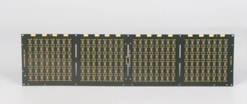
LGA (Land Grid Array) packaging is a type of integrated circuit packaging where the connection between the chip and the PCB (Printed Circuit Board) is made through an array of metallic pads rather than through pins. Unlike traditional pin grid arrays, LGA packages have no pins but instead have pads on the bottom surface, allowing for a more compact design and increased signal density.
Structure
The structure of an LGA package typically consists of the integrated circuit (IC) mounted on a substrate, with the bottom surface featuring an array of metallic pads. These pads serve as the interface for soldering the package to the PCB. The substrate may be made of materials such as FR4 (Fiberglass Reinforced Epoxy) or ceramics, providing mechanical support and electrical insulation for the IC.
Materials
The materials used in manufacturing LGA packaging play a crucial role in ensuring its performance and reliability. Common materials include:
– Substrate: Typically made of FR4, ceramics, or other high-performance materials to provide mechanical support and electrical insulation.
– Metallic Pads: Made of materials like copper or gold-plated copper to facilitate soldering and ensure reliable electrical connections.
– Solder Balls: Used for attaching the package to the PCB, solder balls are typically made of lead-free alloys to comply with environmental regulations and ensure solder joint integrity.
These materials are selected based on their thermal, mechanical, and electrical properties to meet the specific requirements of LGA packaging in different applications.
Advantages of LGA Packaging
Thermal Performance
LGA packaging offers significant thermal advantages over other packaging types due to its design. The absence of through-hole pins reduces thermal resistance between the integrated circuit and the PCB, allowing for more efficient heat dissipation. Additionally, the large surface area of the metallic pads facilitates better thermal conduction, enabling heat to spread evenly across the package. This results in lower operating temperatures for the integrated circuit, enhancing its reliability and longevity. Compared to pin grid array (PGA) or dual in-line package (DIP), LGA packaging minimizes the risk of thermal stress-induced failures, making it ideal for high-power applications and devices requiring robust thermal management.
Electrical Performance
The impact of LGA packaging on electrical performance is significant, primarily attributed to its reduced parasitic inductance and capacitance. The shorter electrical pathways between the integrated circuit and the PCB pads result in lower impedance and improved signal integrity. This leads to faster signal transmission rates, reduced electromagnetic interference (EMI), and enhanced overall electrical performance of the device. Furthermore, LGA packaging allows for closer spacing between pads, enabling higher pin density and increased I/O (Input/Output) count without compromising electrical characteristics. These advantages make LGA packaging well-suited for high-speed digital and analog applications, including microprocessors, FPGAs (Field-Programmable Gate Arrays), and communication interfaces.
Serviceability
LGA packaging offers convenience and ease of serviceability, particularly during repair and maintenance tasks. Unlike surface-mount packages like QFN or BGA, LGA packages can be easily removed and replaced without the need for specialized equipment such as rework stations or reflow ovens. The absence of solder balls underneath the package simplifies rework procedures, allowing technicians to access and replace faulty components more efficiently. Additionally, LGA packages provide better visual inspection of solder joints, enabling quick identification of defects or soldering issues. This enhances the reliability and serviceability of electronic devices, reducing downtime and repair costs in manufacturing and field applications.
Comparison of LGA Packaging with Other Packaging Types
LGA vs. BGA
LGA (Land Grid Array) packaging and BGA (Ball Grid Array) packaging are two common types of surface-mount packaging used in electronic devices, each with its own set of characteristics and application scenarios.
Differences:
1. Connection Method: LGA packaging uses an array of metallic pads for connection, while BGA packaging uses solder balls.
2. Accessibility: LGA packages have exposed pads, making them easier to inspect and rework compared to BGA packages, where the solder balls are hidden underneath.
3. Thermal Performance: LGA packages typically offer better thermal performance due to the larger surface area for heat dissipation compared to BGA packages.
4. Cost: BGA packaging may be more cost-effective for high pin-count applications due to simpler manufacturing processes.
Application Scenarios:
– LGA packaging is often preferred for applications requiring frequent rework or inspection, such as prototyping and testing.
– BGA packaging is commonly used in high-density applications where space is limited and a large number of I/O connections are required, such as microprocessors and memory modules.
LGA vs. QFN
LGA (Land Grid Array) packaging and QFN (Quad Flat No-Lead) packaging are both surface-mount packages widely used in electronic devices, each offering unique features and advantages.
Contrast:
1. Package Design: LGA packages have exposed pads on the bottom surface, while QFN packages have exposed leads on the sides.
2. Size: QFN packages are typically smaller and have a lower profile compared to LGA packages, making them suitable for applications with strict space constraints.
3. Thermal Performance: LGA packages generally offer better thermal performance due to the larger surface area for heat dissipation compared to QFN packages.
4. Lead Configuration: QFN packages have leads arranged around the perimeter of the package, while LGA packages have pads arranged in a grid pattern on the bottom surface.
Pros and Cons:
– LGA packaging provides better accessibility for inspection and rework but may require more PCB space due to the larger footprint.
– QFN packaging offers smaller size and lower profile, making it ideal for compact devices, but may have limitations in thermal dissipation and accessibility for rework.
Application Considerations:
– LGA packaging is suitable for applications requiring high thermal performance and ease of rework, such as power amplifiers and RF modules.
– QFN packaging is preferred for compact and space-constrained applications, such as mobile devices and IoT (Internet of Things) sensors.
Applications of LGA Packaging
Electronics Products
LGA (Land Grid Array) packaging finds extensive applications in a wide range of electronic products due to its versatility, reliability, and performance characteristics. Some examples include:
1. Microprocessors and Microcontrollers: LGA packaging is commonly used for microprocessors and microcontrollers in computers, laptops, servers, and embedded systems. Its thermal efficiency and high pin density make it ideal for high-performance computing applications.
2. Graphics Processing Units (GPUs): High-end GPUs utilized in gaming consoles, graphics cards for PCs, and professional workstations often employ LGA packaging. The thermal advantages of LGA packaging help dissipate heat generated by the GPU’s intensive processing tasks.
3. Networking Equipment: LGA packaging is prevalent in networking equipment such as routers, switches, and network interface cards (NICs). These devices require high-speed data processing and reliable connections, making LGA packaging a suitable choice.
4. Wireless Communication Devices: LGA packaging is used in wireless communication devices like smartphones, tablets, and IoT devices. Its compact size and thermal efficiency make it suitable for integrating complex wireless components in portable devices.
Industrial Applications
In the industrial sector, LGA (Land Grid Array) packaging plays a crucial role in various applications where reliability, durability, and performance are paramount. Some industrial use cases include:
1. Automotive Electronics: LGA packaging is utilized in automotive electronics for applications such as engine control units (ECUs), advanced driver-assistance systems (ADAS), and infotainment systems. Its ability to withstand harsh environmental conditions and high temperatures makes it suitable for automotive applications.
2. Industrial Automation: LGA packaging is employed in industrial automation systems for PLCs (Programmable Logic Controllers), motor drives, and robotics. Its high-speed signal processing capabilities and robust construction ensure reliable operation in demanding industrial environments.
3. Power Electronics: LGA packaging is used in power electronics applications such as inverters, converters, and power supplies. Its thermal efficiency and high current-carrying capacity make it suitable for handling high-power applications in industrial settings.
Soldering Techniques for LGA Packaging
Soldering Methods
Soldering LGA (Land Grid Array) packaging requires precision and care to ensure reliable electrical connections and mechanical stability. Several soldering methods are commonly used for LGA packaging, including:
1. Reflow Soldering: Reflow soldering is the most common method for soldering LGA packages to printed circuit boards (PCBs). In this process, solder paste is applied to the pads on the PCB, and the LGA package is carefully positioned over the pads. The assembly is then heated in a reflow oven, melting the solder paste and forming the solder joints between the LGA pads and PCB pads.
2. Wave Soldering: Wave soldering is another method used for soldering LGA packages, particularly for through-hole LGA packages. In this process, the PCB with LGA packages mounted on it is passed over a wave of molten solder. The solder wets the exposed pads on the bottom of the LGA package, forming solder joints.
3. Hand Soldering: Hand soldering may be necessary for rework or repair of LGA packages. Specialized soldering irons with fine tips are used to apply solder to individual pads on the LGA package. Care must be taken to ensure proper alignment and solder flow to prevent solder bridges or cold joints.
Considerations
When soldering LGA packaging, several key points and techniques should be considered to ensure successful soldering and avoid issues such as solder bridging, insufficient solder, or damage to the components:
1. Solder Paste Quality: Use high-quality solder paste with the appropriate particle size and flux composition to ensure good wetting and solder joint formation during reflow soldering.
2. Stencil Design: Ensure the stencil used for applying solder paste to the PCB has the correct aperture sizes and alignment for the LGA pads to achieve proper solder deposition.
3. Temperature Profile: Optimize the temperature profile during reflow soldering to ensure thorough solder reflow without overheating the components or the PCB.
4. Component Alignment: Ensure accurate component placement and alignment during soldering to prevent misalignment or short circuits between adjacent pads.
5. Solder Joint Inspection: Conduct visual inspection and electrical testing of solder joints after soldering to verify their integrity and reliability.
6. Thermal Management: Implement proper thermal management techniques during soldering to prevent overheating of sensitive components and ensure uniform heating of the assembly.
By adhering to these considerations and employing appropriate soldering techniques, reliable solder joints can be achieved for LGA packaging, ensuring the performance and longevity of electronic devices.
FAQs about lga package
An LGA package, short for Land Grid Array package, is a type of integrated circuit packaging where the connection between the chip and the PCB (Printed Circuit Board) is made through an array of metallic pads on the bottom surface of the package. Unlike traditional pin grid arrays, LGA packages have no pins but instead feature pads, facilitating a more compact design and increased signal density.
The difference between LGA (Land Grid Array) and BGA (Ball Grid Array) packages lies primarily in their connection methods and package design. LGA packages use an array of metallic pads for connection, while BGA packages use solder balls. Additionally, LGA packages typically have exposed pads on the bottom surface, making them easier to inspect and rework compared to BGA packages, where the solder balls are hidden underneath.
An LGA processor package refers to a microprocessor packaged using the LGA (Land Grid Array) packaging technology. In this configuration, the microprocessor’s connection to the PCB (Printed Circuit Board) is facilitated by an array of metallic pads on the bottom surface of the package. LGA processor packages are commonly used in various computing devices, including computers, laptops, servers, and embedded systems, due to their thermal efficiency, compact size, and high pin density.
The difference between LGA (Land Grid Array) and QFN (Quad Flat No-Lead) packages lies in their package design and lead configuration. LGA packages feature pads arranged in a grid pattern on the bottom surface, whereas QFN packages have leads arranged around the perimeter of the package. Additionally, LGA packages typically offer better thermal performance due to their larger surface area for heat dissipation compared to QFN packages.

