
Understanding Leadframe vs Substrate: Roles in Packaging
As semiconductor devices become smaller, faster, and more energy-efficient, packaging technology has quietly undergone a transformation. The shift from leadframe-based IC packaging to substrate-based packaging represents one of the most critical shifts in semiconductor packaging.
This article will delve into leadframe and substrate packaging—what they are, how they are manufactured, and the advantages they offer in modern semiconductor manufacturing.
Understanding Leadframe vs Substrate Evolution
Traditional leadframe packages such as SOICs, QFPs, and QFNs have served the industry for decades, offering low-cost and reliable interconnections. However, as chip I/O counts and signal speeds increased, engineers required finer interconnect density and better electrical performance.
This led to the rise of package substrates, which replaced stamped metal frames with multilayer organic or inorganic laminates capable of routing thousands of signals in compact layouts. Today, the leadframe vs substrate debate is no longer just about cost — it’s about balancing performance, thermal efficiency, and manufacturability.
Get a Quotation For Leadframe vs Substrate Now
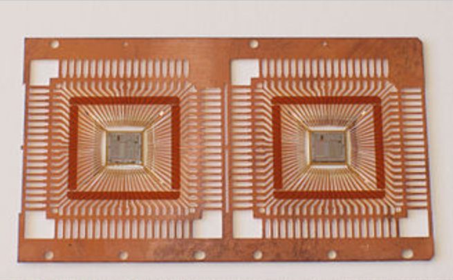
What Is a Leadframe? Structure, Function, and Plating
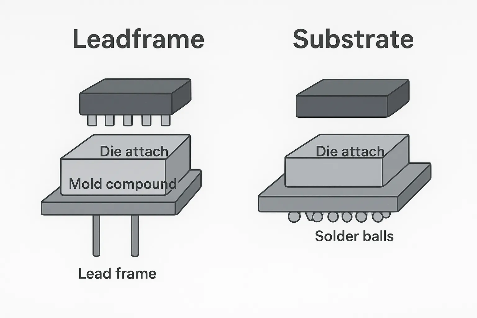
A leadframe is a thin sheet of metal, typically made from copper alloy or Fe-Ni alloy (Alloy 42), designed to support and interconnect a semiconductor die. It acts as both the mechanical foundation and electrical interface between the chip and the external pins or leads.
Functions of a Leadframe
-
Mechanical support: Holds the die in place during wire bonding and molding.
-
Electrical connection: Conducts signals from the die to the external pins.
-
Thermal management: Provides a direct path for heat dissipation.
Leadframe Plating
Surface plating improves wire bondability and solderability. Common plating types include:
-
Ag (Silver): Excellent conductivity, but tarnishes easily.
-
NiPdAu: Preferred for wire bonding and oxidation resistance.
-
Sn (Tin): Used for cost-effective solder interfaces.
Leadframe packaging dominates in low-cost, high-volume products — power ICs, analog devices, and automotive components.
Get a Quotation For Leadframe vs Substrate Now
What Is a Substrate in Semiconductor Packaging?
In contrast, a substrate in semiconductor packaging is a multilayer interconnect structure that electrically connects the silicon die to the printed circuit board (PCB). It serves as a miniature circuit board within the package.
Substrate vs PCB
-
PCB: Designed for large-scale interconnections between components.
-
Substrate: Built for fine-pitch, high-density routing under a single die or multi-chip module.
Substrate vs Wafer
While the wafer is the silicon base where transistors are formed, the substrate is the platform that redistributes the die’s tiny I/O pads into larger solder bumps for board-level mounting.
Common Substrate Materials
-
BT resin (Bismaleimide Triazine) – cost-effective, good thermal reliability.
-
ABF (Ajinomoto Build-up Film) – high-frequency performance for advanced flip-chip packages.
-
Ceramic or Glass substrates – used in high-end applications (AI, HPC).
Get a Quotation For Leadframe vs Substrate Now
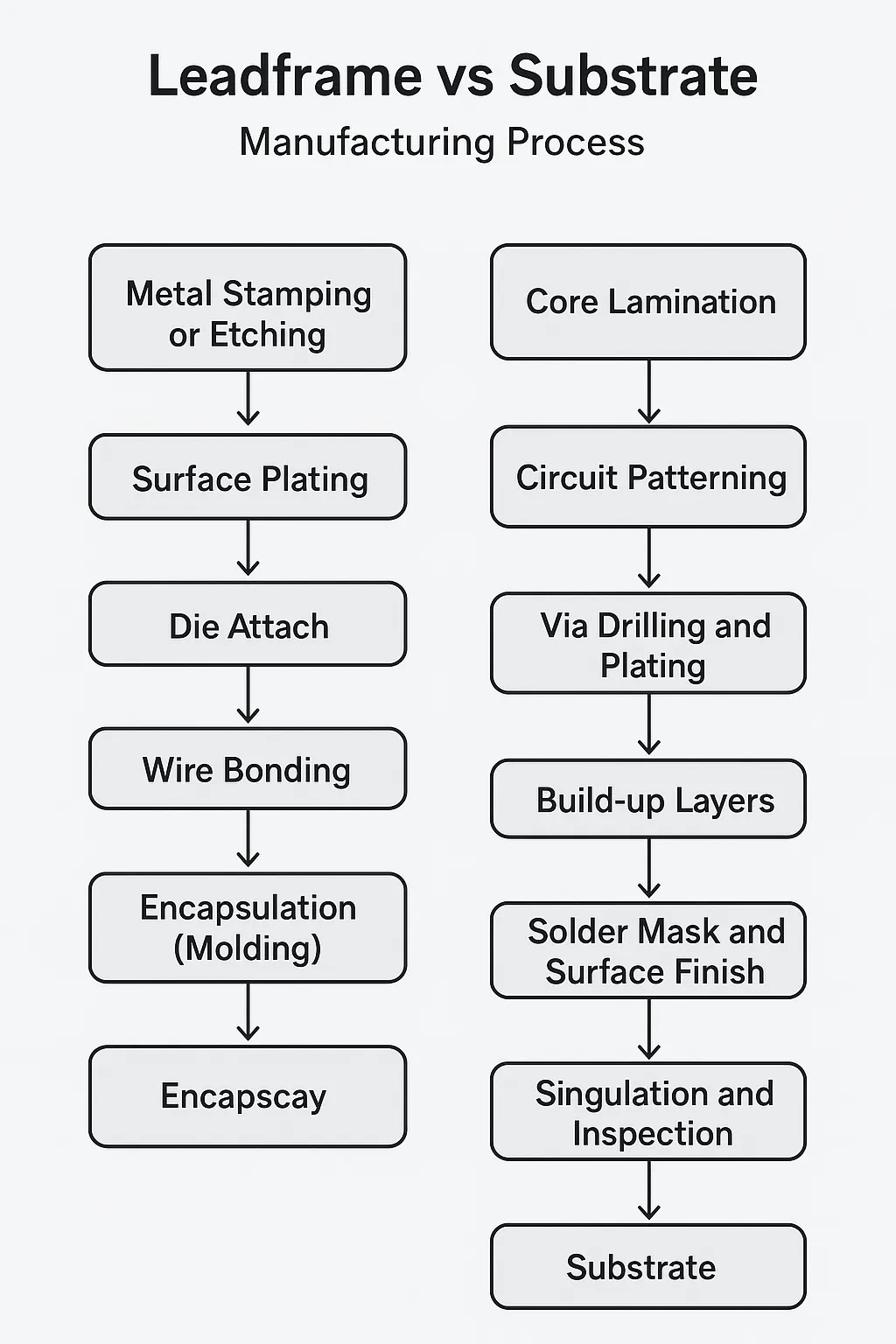
Leadframe vs Substrate: Manufacturing Process Flow
Leadframe Process
-
Metal stamping or etching to form lead patterns.
-
Surface plating with NiPdAu, Ag, or Sn.
-
Die attach using conductive epoxy or solder.
-
Wire bonding to connect die pads to leads.
-
Molding encapsulation with epoxy compound.
-
Trimming and forming to separate leads and shape the package.
IC Substrate Process
-
Core lamination using BT or ABF resin.
-
Photolithography & etching to form fine copper traces.
-
Via drilling and Cu plating for layer interconnection.
-
Build-up dielectric and RDL (Redistribution Layer) formation.
-
Solder mask coating and surface finishing.
-
Singulation and final inspection.
Get a Quotation For Leadframe vs Substrate Now
Leadframe vs Substrate in Wafer-Level and Flip-Chip Packaging
Wafer-Level Packaging (WLP) and Flip-Chip technologies represent the next step beyond leadframe-based assembly.
-
WLCSP (Wafer-Level Chip Scale Package): The entire package is formed directly on the wafer before dicing — no substrate or leadframe needed.
-
Flip-Chip BGA / FC-CSP: The die is flipped and mounted directly onto the substrate using solder bumps, achieving shorter interconnects and better electrical performance.
Meanwhile, Molded Interconnect Substrate (MIS) technology integrates 3D wiring and embedded components, blurring the boundary between packaging and substrate design.
These modern architectures show how the leadframe vs substrate choice defines electrical performance and miniaturization capabilities.
Get a Quotation For Leadframe vs Substrate Now
Key Technical Comparison: Leadframe vs Substrate
| Parameter | Leadframe | Substrate |
|---|---|---|
| Material | Cu, Alloy 42 | BT, ABF, Glass, Ceramic |
| Layers | Single metal | Multilayer (2–10+) |
| Interconnect Type | Wire bond | Flip-chip / RDL |
| Pitch | >80 μm | <20 μm |
| Thermal Conductivity | Excellent | Moderate |
| Electrical Performance | Moderate | Superior (shorter signal paths) |
| Cost | Low | High |
| Package Examples | QFN, SOIC, TO, DIP | BGA, FC-CSP, SiP |
From a design standpoint, leadframes are unmatched for heat dissipation and cost efficiency, while substrates excel in signal integrity, miniaturization, and multilayer routing.
Get a Quotation For Leadframe vs Substrate Now
Major Manufacturers and Market Overview
Semiconductor Substrate Manufacturers
-
ALCANTA PCB – A leading provider of custom package substrate and advanced PCB manufacturing services. ALCANTA specializes in high-density interconnect (HDI) substrates, embedded copper-core technology, and fine-line routing for power, RF, and SiP applications — bridging the gap between leadframe vs substrate technologies.
-
Ibiden – Supplies advanced ABF substrates for Intel and Nvidia high-performance processors.
-
Shinko Electric – Expert in BT-based package substrates widely used in consumer and communication ICs.
-
Samsung Electro-Mechanics – Expanding production of organic and glass substrates for next-generation chip packaging.
-
Toppan, Unimicron, Nan Ya PCB – Industry leaders in FC-BGA substrate manufacturing for AI, data center, and server applications.
Leadframe Manufacturers
-
Mitsui High-tec – Produces high-precision stamped and etched leadframes, essential for power and automotive ICs.
-
ASM Pacific, SDI, Chang Wah Tech – Major suppliers of leadframes for analog, discrete, and high-reliability packages.
As semiconductor packaging continues to evolve, many companies now integrate both leadframe and substrate production capabilities — enabling hybrid solutions such as molded array packages, system-in-package (SiP), and advanced power modules that blend performance and cost advantages.
Contact Us Now
FQAs Abut Leadframe vs Substrate
What is the purpose of the Leadframe?
The Leadframe is a key component in semiconductor packaging, providing electrical connections between the IC’s internal components and external pins or leads. It helps establish the path for electrical signals and power to flow in and out of the IC. Additionally, the Leadframe aids in heat dissipation and mechanical support during the packaging process, ensuring that the IC is securely connected and can function efficiently.
What is the difference between substrate and interposer?
The Substrate and Interposer both play crucial roles in semiconductor packaging, but they differ in their functions and applications:
- Substrate: A Substrate provides mechanical support, electrical interconnections, and thermal management for the integrated circuit. It is often used in high-density packaging and provides the base for mounting the IC and connecting it to external components through pads or traces.
- Interposer: An Interposer is a specialized layer that sits between the Substrate and the IC. It is primarily used to connect multiple chips in 3D packaging or multichip modules (MCM). The Interposer provides additional interconnectivity and can also aid in thermal management and signal integrity.
What is a substrate in a semiconductor?
In a semiconductor, a Substrate refers to the base material that supports and connects the semiconductor chip or device. It provides both mechanical support and the necessary electrical connections between the semiconductor device and the external components. It is typically made from materials like ceramics, epoxy-based PCBs, or BT resin. The Substrate also helps manage heat dissipation and ensures the long-term reliability of the device in electronic applications.
What is a substrate in packaging?
In packaging, a Substrate is the foundational material used to connect the semiconductor chip to the external world. It provides a stable platform for mounting the chip and routes the electrical signals from the chip to the external leads or pins. Substrates in packaging are designed to minimize signal loss, enhance heat dissipation, and support high-density interconnects. Common materials for packaging substrates include ceramics, epoxy laminates, and BT resin, depending on the required thermal, electrical, and mechanical properties.

