
JEDEC QFN: Compact Design, Powerful Performance
In the ever-evolving landscape of electronics manufacturing, adherence to standardized packaging formats is paramount. Among these standards, the JEDEC QFN package standard stands as a cornerstone. This guide aims to delve into the intricacies of this ubiquitous packaging solution, shedding light on its design, advantages, and applications. Understanding such standards is not merely a matter of compliance; it is the foundation upon which reliable, interoperable, and innovative electronic devices are built. As technology advances and demands for smaller, more efficient components grow, familiarity with packaging standards like JEDEC QFN becomes indispensable for engineers, designers, and manufacturers alike, ensuring seamless integration and optimal performance in the complex ecosystem of electronic devices.
What is JEDEC QFN Package Standard?
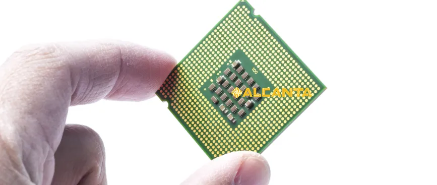
The JEDEC QFN (Quad Flat No-leads) package standard, established by the Joint Electron Device Engineering Council, represents a widely adopted packaging solution in the semiconductor industry. This standard delineates the design, dimensions, and specifications for QFN packages, ensuring uniformity and compatibility across various manufacturers.
Overview of Design, Features, and Applications:
Design: QFN packages typically feature a flat surface with exposed leads arranged in a grid pattern on the bottom side of the package. Unlike traditional packages with protruding leads, QFN packages have leads that are flush with or slightly recessed into the package body, hence the term “no-leads.” This design offers several advantages, including reduced package size, improved thermal performance, and enhanced electrical characteristics.
Features: One distinctive feature of QFN packages is their leadframe-based construction, which allows for efficient heat dissipation and high electrical conductivity. Additionally, QFN packages often incorporate features such as thermal pads, which facilitate effective heat transfer to the PCB (Printed Circuit Board), and exposed paddle designs, which enhance electrical performance and solder joint reliability.
Applications: The versatility of QFN packages makes them suitable for a wide range of applications, including integrated circuits (ICs), microcontrollers, RF (Radio Frequency) devices, and power management components. Their compact size, excellent thermal characteristics, and compatibility with surface-mount assembly processes make QFN packages particularly well-suited for portable electronics, automotive systems, consumer devices, and industrial equipment.
Overall, the JEDEC QFN package standard serves as a cornerstone in modern electronics manufacturing, providing designers and manufacturers with a standardized, reliable, and efficient packaging solution for a diverse array of semiconductor devices. Understanding the intricacies of this standard is essential for ensuring compatibility, reliability, and performance in today’s rapidly evolving electronics industry.
Advantages of QFN Package
The QFN (Quad Flat No-leads) package offers numerous advantages over traditional packaging solutions, making it a preferred choice for many semiconductor applications. Here’s a detailed exploration of its key benefits:
1. Compact Size: One of the most significant advantages of QFN packages is their compact size. With no leads protruding from the package, QFNs have a smaller footprint compared to packages with traditional lead frames. This compactness allows for higher component density on PCBs (Printed Circuit Boards), enabling the design of smaller and more lightweight electronic devices. It’s particularly advantageous in applications where space is limited, such as mobile devices, wearables, and IoT (Internet of Things) devices.
2. Better Thermal Performance: QFN packages excel in thermal management due to their unique design. The exposed metal pad on the bottom of the package serves as a heat sink, efficiently dissipating heat generated by the integrated circuit. Furthermore, the absence of leads minimizes thermal resistance between the package and the PCB, improving heat transfer. This superior thermal performance enhances the reliability and longevity of electronic devices, especially in applications that require high power dissipation or operate in demanding environments.
3. Improved Electrical Characteristics: QFN packages offer enhanced electrical characteristics compared to traditional leaded packages. The shorter electrical paths and reduced parasitic capacitance and inductance contribute to lower signal propagation delays, improved signal integrity, and higher operating frequencies. These attributes are particularly beneficial in high-speed digital and RF (Radio Frequency) applications, where signal integrity and transmission performance are critical.
4. Enhanced Mechanical Stability: The absence of leads in QFN packages results in improved mechanical stability and robustness. Since the leads are integrated directly into the package substrate, there’s less susceptibility to damage from mechanical stress, vibration, or thermal cycling. This enhanced durability increases the reliability and ruggedness of electronic devices, making QFN packages suitable for automotive, aerospace, and industrial applications where reliability is paramount.
5. Cost-Effectiveness: QFN packages offer cost advantages over some other packaging options. Their simplified design and manufacturing process result in lower production costs, making them a cost-effective solution for high-volume applications. Additionally, their compatibility with surface-mount assembly processes further reduces assembly time and costs.
Overall, the compact size, superior thermal performance, improved electrical characteristics, enhanced mechanical stability, and cost-effectiveness of QFN packages make them an attractive choice for a wide range of electronic applications, driving innovation and efficiency in the semiconductor industry.
Disadvantages of QFN Package
While QFN (Quad Flat No-leads) packages offer numerous advantages, they also come with certain drawbacks that need to be considered in electronic design and manufacturing processes. Here’s a detailed exploration of some of the key disadvantages:
1. Difficulty in Rework: One significant drawback of QFN packages is the challenge associated with rework and repair. Unlike traditional leaded packages where leads can be easily accessed and reworked, QFN packages have no external leads, making it difficult to access and replace individual components. Reworking QFN packages often requires specialized equipment and techniques, such as hot air rework stations or infrared reflow systems, which can increase repair time and costs. Additionally, the risk of damaging adjacent components during rework is higher, further complicating the process.
2. Reliability Issues Due to Solder Joints: Another potential drawback of QFN packages is the reliability of solder joints. Since QFN packages rely on surface-mount soldering techniques, the integrity of solder joints is critical for ensuring electrical connectivity and mechanical stability. However, factors such as inadequate solder volume, uneven heating during soldering, or insufficient solder wetting can lead to solder joint defects, such as voids, cracks, or incomplete wetting. These defects can compromise the long-term reliability of the package, potentially leading to electrical failures or intermittent connections over time, especially in applications exposed to thermal cycling, mechanical stress, or harsh environmental conditions.
3. Limited Accessibility for Testing: QFN packages often feature a large exposed thermal pad on the bottom side, which provides efficient heat dissipation but also limits accessibility for testing and probing. Unlike leaded packages where test points are readily accessible, testing QFN packages may require specialized fixtures or techniques to make contact with internal nodes or signal traces, adding complexity and cost to the testing process. This limited accessibility can hinder debugging, troubleshooting, and quality assurance efforts during product development and manufacturing.
4. Risk of Package Warpage: QFN packages are susceptible to package warpage during assembly processes, especially during solder reflow. Variations in substrate material, assembly temperatures, and cooling rates can cause uneven thermal expansion and contraction, leading to package warpage or deformation. Package warpage can result in poor solder wetting, misalignment of components, or mechanical stress on solder joints, compromising the overall reliability and performance of the package.
While QFN packages offer numerous advantages, including compact size, improved thermal performance, and enhanced electrical characteristics, it’s essential to consider these potential drawbacks and implement appropriate design, assembly, and testing practices to mitigate risks and ensure the reliability and performance of electronic devices.
Standard Size of QFN Packages
JEDEC (Joint Electron Device Engineering Council) standardizes the dimensions and specifications of QFN (Quad Flat No-leads) packages to ensure interoperability and compatibility across different manufacturers. While specific dimensions may vary depending on the application and package variant, there are typical dimensions and variations commonly encountered in JEDEC standard QFN packages:
1. Body Size: The body size of a QFN package refers to the dimensions of the outer edges of the package. Common body sizes for JEDEC standard QFN packages range from 2 mm x 2 mm to 12 mm x 12 mm or larger. However, smaller and larger sizes are also available for specialized applications.
2. Lead Pitch: Lead pitch refers to the distance between adjacent leads on the bottom surface of the QFN package. Standard lead pitches typically range from 0.4 mm to 1.0 mm, although finer pitches may be available for high-density applications requiring closer lead spacing.
3. Lead Count: QFN packages come in various lead counts to accommodate different integrated circuit designs and requirements. Standard lead counts range from as few as 4 leads to over 100 leads, with common configurations including 4×4, 5×5, 6×6, 8×8, and 10×10 arrangements.
4. Lead Width and Thickness: The width and thickness of the leads on a QFN package contribute to the overall electrical performance and reliability of the package. Standard lead widths typically range from 0.2 mm to 0.5 mm, while lead thicknesses may vary from 0.1 mm to 0.3 mm, depending on the package size and lead pitch.
5. Exposed Pad Size: Many QFN packages feature an exposed thermal pad on the bottom surface, which aids in heat dissipation and electrical grounding. The size of the exposed pad can vary significantly depending on the package size and thermal requirements of the application. Typical exposed pad sizes range from 1 mm x 1 mm to 6 mm x 6 mm or larger, with variations in shape (e.g., square, rectangular) to accommodate different assembly and thermal management needs.
6. Thickness: The overall thickness of a QFN package, including the package body and leadframe, is another important dimension that can influence assembly, reliability, and thermal performance. Standard thicknesses range from around 0.5 mm to 1.5 mm, with thinner packages offering advantages in terms of space savings and thermal conductivity, while thicker packages provide increased mechanical strength and durability.
Understanding the typical dimensions and variations in size for JEDEC standard QFN packages is essential for designers, manufacturers, and assembly engineers to ensure proper component selection, PCB layout, and assembly processes, ultimately leading to reliable and high-performance electronic devices.
Full Form of QFN Package
QFN stands for Quad Flat No-leads, which provides insight into the key features and design characteristics of this popular semiconductor packaging format.
Quad: The term “Quad” in QFN refers to the four sides of the package’s exterior shape, typically rectangular or square. This configuration allows for a compact footprint while accommodating a relatively large number of leads compared to traditional dual in-line packages (DIPs) or single in-line packages (SIPs).
Flat: The “Flat” aspect of QFN highlights the package’s low profile design, characterized by a thin and flat body. This low profile is achieved by embedding the integrated circuit die directly into the package substrate, eliminating the need for leads extending beyond the package body.
No-leads: Perhaps the most distinctive feature of QFN packages is the absence of external leads protruding from the package body. Instead, electrical connections are made via metal pads located on the bottom surface of the package, which are soldered directly to corresponding pads on the PCB (Printed Circuit Board). This “no-leads” configuration streamlines the assembly process, reduces the risk of lead damage or misalignment, and enhances electrical performance by minimizing parasitic inductance and capacitance.
In summary, the abbreviation QFN encapsulates the essential characteristics of this packaging format: a compact, low-profile package with no external leads, making it a versatile and widely used solution for modern semiconductor devices.
Comparison with Other Package Standards
When considering semiconductor packaging options, engineers often evaluate various standards to determine the most suitable solution for their specific application requirements. Here’s a brief comparison between the QFN (Quad Flat No-leads) package and other popular packaging standards like BGA (Ball Grid Array) and SOP (Small Outline Package):
1. QFN vs. BGA (Ball Grid Array):
QFN Package:
– QFN packages feature leads that are flush with or slightly recessed into the package body, facilitating surface-mount assembly and improving thermal performance.
– The absence of external leads reduces the risk of lead damage and enhances electrical performance by minimizing parasitic inductance and capacitance.
– QFN packages offer a lower profile compared to many BGA packages, making them suitable for applications with height constraints.
BGA Package:
– BGA packages consist of a grid array of solder balls on the bottom surface, providing reliable electrical connections and simplifying PCB routing.
– BGA packages offer excellent thermal dissipation capabilities due to the large number of solder balls that act as heat sinks, making them suitable for high-power applications.
– BGA packages typically have a higher pin count and larger package size compared to QFN packages, allowing for increased integration and connectivity.
2. QFN vs. SOP (Small Outline Package):
QFN Package:
– QFN packages offer a smaller footprint and higher lead count compared to many SOP packages, enabling greater component density and miniaturization of electronic devices.
– The absence of leads protruding from the package body simplifies the assembly process and reduces the risk of lead damage during handling.
– QFN packages generally provide better thermal performance and electrical characteristics compared to SOP packages, particularly in high-frequency applications.
SOP Package:
– SOP packages feature leads that extend from the sides of the package, providing ease of soldering and inspection during assembly.
– SOP packages are available in various configurations, including SOP, SSOP (Shrink Small Outline Package), and TSOP (Thin Small Outline Package), offering flexibility in terms of package size and lead count.
– SOP packages are commonly used in consumer electronics and industrial applications where cost-effectiveness and ease of assembly are priorities.
In summary, the choice between QFN, BGA, and SOP packages depends on factors such as package size, lead count, thermal requirements, electrical performance, and assembly considerations. Each package standard offers unique advantages and trade-offs, allowing engineers to select the most appropriate solution based on the specific needs of their design.
JEDEC Standard BGA Package Size
The JEDEC (Joint Electron Device Engineering Council) standardizes the dimensions and specifications of BGA (Ball Grid Array) packages to ensure interoperability and compatibility across different manufacturers. The size specifications of JEDEC standard BGA packages vary depending on factors such as ball pitch, ball count, and package dimensions. Here’s a detailed overview:
1. Ball Pitch: The ball pitch refers to the distance between the centers of adjacent solder balls on the bottom surface of the BGA package. Common ball pitches for JEDEC standard BGA packages range from 0.4 mm to 1.27 mm, with finer pitches available for high-density applications requiring closer ball spacing.
2. Ball Count: BGA packages come in various ball counts to accommodate different integrated circuit designs and requirements. Standard ball counts range from as few as 4 balls to several hundred balls, with common configurations including 4×4, 6×6, 8×8, 10×10, and larger grid arrays.
3. Package Dimensions: The overall dimensions of JEDEC standard BGA packages can vary depending on the package size and ball pitch. Typical package sizes range from 5 mm x 5 mm to 40 mm x 40 mm or larger, with variations in shape (e.g., square, rectangular) to accommodate different die sizes and assembly requirements.
Applications of JEDEC Standard BGA Packages
JEDEC standard BGA packages find widespread use in a variety of electronic applications due to their compact size, high pin count, and robust electrical connections. Some common applications include:
1. Consumer Electronics: BGA packages are commonly used in smartphones, tablets, laptops, and other consumer electronics devices where space constraints and high-performance requirements drive the need for compact and efficient packaging solutions.
2. Networking and Communication Devices: BGA packages are prevalent in networking equipment, routers, switches, and communication devices due to their ability to handle high-speed data transmission and provide reliable electrical connections for complex circuitry.
3. Computing Systems: BGA packages are widely used in central processing units (CPUs), graphics processing units (GPUs), memory modules, and other computing components to achieve high integration levels, efficient thermal management, and reliable interconnectivity.
4. Automotive Electronics: BGA packages are increasingly utilized in automotive electronic systems such as engine control units (ECUs), infotainment systems, advanced driver assistance systems (ADAS), and in-vehicle networking modules due to their ability to withstand harsh environmental conditions and temperature extremes.
5. Industrial Applications: BGA packages are employed in various industrial applications, including automation equipment, control systems, robotics, and instrumentation, where reliability, durability, and high-performance packaging are essential for long-term operation in demanding environments.
Overall, JEDEC standard BGA packages play a vital role in modern electronics manufacturing, enabling designers and manufacturers to achieve high levels of integration, performance, and reliability in a wide range of applications across diverse industries.
FAQs about jedec qfn package standard
The disadvantages of QFN (Quad Flat No-leads) packages include difficulty in rework and repair due to the absence of external leads, potential reliability issues related to solder joints, limited accessibility for testing and probing, and the risk of package warpage during assembly processes.
The standard size of QFN packages varies depending on the specific application and requirements. However, typical dimensions for JEDEC standard QFN packages range from 2 mm x 2 mm to 12 mm x 12 mm or larger, with variations in lead pitch, lead count, and package thickness.
QFN stands for Quad Flat No-leads, which describes the key features of this semiconductor packaging format. It features a flat surface with exposed leads arranged in a grid pattern on the bottom side of the package, and unlike traditional packages, it lacks external leads protruding from the package body.
The size of a JEDEC standard BGA package can vary depending on factors such as ball pitch, ball count, and package dimensions. Typical package sizes range from 5 mm x 5 mm to 40 mm x 40 mm or larger, with variations in shape (e.g., square, rectangular) to accommodate different die sizes and assembly requirements.

