
Decoding IC Package Types: Advantages and Disadvantages
Integrated Circuit (IC) packaging plays a critical role in the performance and reliability of electronic devices. At its core, IC packaging involves enclosing the semiconductor material in a protective case that provides mechanical support, protects against physical damage and environmental hazards, and ensures efficient electrical connections to the circuit board. This packaging is essential not only for safeguarding the delicate IC components but also for enabling proper heat dissipation, which is crucial for maintaining optimal performance and longevity.
The purpose of this article is to provide a comprehensive overview of the most common IC package types and their specific applications. By understanding the different IC package types, from traditional Dual In-line Packages (DIP) to modern Ball Grid Arrays (BGA) and Chip Scale Packages (CSP), readers will gain insights into their unique characteristics, advantages, and ideal use cases. This knowledge is invaluable for engineers, designers, and enthusiasts looking to select the appropriate IC packages for their electronic projects.
What is IC Packaging? Exploring IC Package Types
Definition
IC packaging is a fundamental aspect of semiconductor technology, encompassing the process of enclosing an integrated circuit (IC) chip within a protective housing. This housing, known as the package, serves as a crucial interface between the delicate semiconductor materials and the external environment. It not only shields the chip from physical damage, moisture, and contaminants but also facilitates electrical connections to the circuit board.
Functions
1. Protection: IC packaging provides essential physical protection to the semiconductor chip, safeguarding it from mechanical stress, environmental hazards, and electrostatic discharge. By encapsulating the chip within a durable housing, packaging ensures its reliability and longevity in various operating conditions.
2. Electrical Connections: Another vital function of IC packaging is to establish and maintain electrical connections between the integrated circuit and other components on the printed circuit board (PCB). The package incorporates conductive leads or terminals that enable the transmission of electrical signals and power between the IC and the rest of the electronic system.
3. Heat Management: Effective heat management is crucial for maintaining the performance and reliability of integrated circuits. IC packaging designs often incorporate features such as heat sinks, thermal pads, and exposed metal areas to dissipate heat generated during operation. By efficiently managing thermal energy, packaging helps prevent overheating and ensures optimal performance of the semiconductor chip.
IC packaging plays a vital role in protecting the chip, facilitating electrical connections, and managing heat, making it an indispensable component in modern electronic devices.
Common IC Package Types
Dual In-line Package (DIP)
Characteristics: The Dual In-line Package (DIP) is characterized by its two parallel rows of pins, which extend perpendicularly from the longer sides of a rectangular housing. This design allows for easy manual soldering and insertion into breadboards and through-hole PCBs, making it ideal for prototyping and small-scale production.
Example Applications: DIP packages were commonly used in early microprocessors, such as the Intel 8088, and in various small-scale integrated circuits like operational amplifiers and simple logic gates. Despite their declining use in mass production due to larger size and lower pin density, they remain popular in educational kits and hobbyist projects.
Small Outline Integrated Circuit (SOIC)
Characteristics: The Small Outline Integrated Circuit (SOIC) features a smaller pin spacing (typically 1.27 mm) and a lower profile compared to DIP, making it more suitable for surface mount technology (SMT). This compact design allows for higher density placement on PCBs, which is crucial in modern electronics where space conservation is key.
Example Applications: SOIC packages are widely used in modern microcontrollers, such as the Atmel ATmega328P, and memory chips like EEPROMs and flash memory. Their compatibility with automated pick-and-place machinery and reflow soldering processes makes them a staple in contemporary electronics manufacturing.
Quad Flat Package (QFP)
Characteristics: The Quad Flat Package (QFP) has pins on all four sides of the square or rectangular housing. This configuration allows for a higher pin count than DIP or SOIC, facilitating high-density mounting. QFP packages are designed for surface mounting and are compatible with automated assembly processes.
Example Applications: QFP packages are commonly found in consumer electronics, including microprocessors and microcontrollers in devices like smartphones and gaming consoles, as well as in computer hardware such as graphics cards and motherboards. Their high pin count and compact design make them ideal for complex integrated circuits.
Ball Grid Array (BGA)
Characteristics: The Ball Grid Array (BGA) package utilizes an array of spherical solder balls on the underside of the package, replacing traditional pins. This design enhances electrical performance and heat dissipation due to shorter electrical paths and a more direct thermal path to the PCB.
Example Applications: BGA packages are used in high-performance processors, including CPUs and GPUs, as well as large memory modules. Their ability to support high pin counts and superior heat management makes them suitable for demanding applications in servers, gaming systems, and advanced computing devices.
Chip Scale Package (CSP)
Characteristics: The Chip Scale Package (CSP) is almost as small as the die itself, making it highly suitable for space-constrained applications. CSPs typically use an array of solder bumps or balls for connections, similar to BGA but on a smaller scale.
Example Applications: CSPs are frequently used in mobile devices, such as smartphones and tablets, as well as in portable electronics like digital cameras and wearable devices. Their minimal footprint and weight are advantageous in devices where compactness is crucial.
Quad Flat No-lead Package (QFN)
Characteristics: The Quad Flat No-lead Package (QFN) lacks external leads and instead uses metal pads or lands on the bottom of the package for electrical connections. This design provides excellent thermal performance and electrical characteristics due to the reduced lead inductance and improved heat dissipation.
Example Applications: QFN packages are suitable for wireless communication modules, RF applications, and other high-frequency circuits. They are commonly found in Bluetooth modules, Wi-Fi chips, and RF transceivers where efficient heat management and electrical performance are critical.
These IC package types each offer unique advantages tailored to specific applications and requirements in modern electronic design, from prototyping and small-scale projects to high-performance computing and compact mobile devices. Understanding these differences is essential for selecting the right package for any given application.
Surface Mount Device (SMD) IC Package Types
Introduction to Surface Mount Technology (SMT)
Surface Mount Technology (SMT) revolutionized the electronics manufacturing industry by allowing components to be mounted directly onto the surface of printed circuit boards (PCBs) rather than being inserted into holes. This method provides several significant advantages:
- Higher Component Density: SMT allows for more components to be placed on both sides of the PCB, leading to more compact and lightweight electronic devices.
- Improved Performance: The shorter leads and reduced lead inductance in SMT result in better electrical performance, which is especially beneficial in high-frequency applications.
- Automated Assembly: SMT components are compatible with automated pick-and-place machines and reflow soldering processes, increasing production speed, consistency, and reducing labor costs.
- Enhanced Reliability: SMT connections tend to be more reliable due to lower susceptibility to mechanical stress and vibration compared to through-hole components.
Application areas for SMT include consumer electronics, telecommunications, automotive electronics, medical devices, and industrial equipment, where compact size, high performance, and production efficiency are critical.
Common SMD Package Types
Small Outline Integrated Circuit (SOIC)
| Parameter | Description |
| Characteristics | Smaller pin spacing, suitable for surface mount technology |
| Pin Spacing | Typically 1.27 mm |
| Mounting Type | Surface mount |
| Applications | Modern microcontrollers, memory chips |
Example Applications: SOIC packages are extensively used in microcontrollers (e.g., Atmel ATmega series) and memory chips (e.g., EEPROMs and flash memory).
Quad Flat Package (QFP)
| Parameter | Description |
| Characteristics | Pins on all four sides, suitable for high-density mounting |
| Pin Count | High (typically ranging from 32 to 304 pins) |
| Mounting Type | Surface mount |
| Applications | Consumer electronics, computer hardware |
Example Applications: QFP packages are found in a variety of consumer electronics, including smartphones, gaming consoles, and computer hardware components like graphics cards and motherboards.
Ball Grid Array (BGA)
| Parameter | Description |
| Characteristics | Uses spherical solder balls on the underside, offering better electrical performance and heat management |
| Pin Count | Very high (typically 100+ balls) |
| Mounting Type | Surface mount |
| Applications | High-performance processors, large memory modules |
Example Applications: BGA packages are commonly used in high-performance CPUs, GPUs, and large memory modules due to their superior electrical and thermal properties.
Chip Scale Package (CSP)
| Parameter | Description |
| Characteristics | Size close to the chip itself, suitable for space-constrained applications |
| Size | Minimal, near-die size |
| Mounting Type | Surface mount |
| Applications | Mobile devices, portable electronics |
Example Applications: CSP packages are frequently found in mobile devices, such as smartphones and tablets, as well as in portable electronics like digital cameras and wearable technology.
Quad Flat No-lead Package (QFN)
| Parameter | Description |
| Characteristics | No external leads, uses bottom contacts, excellent thermal performance |
| Pin Count | Moderate (typically ranging from 8 to 100 pins) |
| Mounting Type | Surface mount |
| Applications | Wireless communication, RF modules |
Example Applications: QFN packages are widely used in wireless communication modules, RF applications, and other high-frequency circuits where efficient heat management and electrical performance are critical.
These SMD package types each bring unique benefits, making them suitable for a wide range of applications in modern electronics. Understanding their characteristics helps in selecting the right package for specific needs, ensuring optimal performance and reliability of electronic devices.
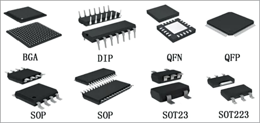
Images of IC Package Types
Below is an image gallery showcasing various IC package types, each representing a different packaging technology used in electronic circuits.
Dual In-line Package (DIP)
Example Analysis: Dual In-line Package (DIP): The image shows a typical DIP package with two parallel rows of pins extending from the sides. Each pin can be easily inserted into a breadboard or through-hole PCB for prototyping and manual soldering. DIP packages are known for their simplicity and ease of use, making them ideal for educational purposes and small-scale projects.

Small Outline Integrated Circuit (SOIC)
Example Analysis: Small Outline Integrated Circuit (SOIC): This image depicts an SOIC package, which has a more compact form factor compared to DIP. The pins extend from the sides with a smaller pitch, suitable for surface mount technology (SMT). SOIC packages are commonly used in applications requiring automated assembly and higher component density on the PCB.

Quad Flat Package (QFP)
Example Analysis: Quad Flat Package (QFP): The QFP shown here features pins on all four sides of the package. This high pin count design supports complex integrated circuits and high-density mounting, making it suitable for advanced consumer electronics and computer hardware. The flat leads are ideal for surface mounting, enhancing the package’s stability and electrical performance.

Ball Grid Array (BGA)
Example Analysis: Ball Grid Array (BGA): The image illustrates a BGA package with an array of solder balls on the underside. These spherical balls provide connections to the PCB, allowing for higher pin density and better electrical performance. BGA packages are used in high-performance applications like processors and memory modules due to their superior heat dissipation capabilities and compact design.

Chip Scale Package (CSP)
Example Analysis: Chip Scale Package (CSP): This image shows a CSP, which is nearly the same size as the die itself. CSP packages are designed for minimal footprint applications, making them perfect for mobile and portable electronics where space is highly constrained. The small size and efficient thermal management of CSPs are advantageous in high-density, compact device designs.
Quad Flat No-lead Package (QFN)
Example Analysis: Quad Flat No-lead Package (QFN): The QFN package in the image lacks external leads and uses metal pads or lands on the bottom for electrical connections. This design improves thermal performance and reduces lead inductance, making QFNs ideal for high-frequency applications and wireless communication modules. The bottom contacts ensure efficient heat dissipation and robust electrical connections.

These images and analyses provide a visual understanding of various IC package types, highlighting their unique characteristics and applications. From the simple and versatile DIP to the high-performance BGA and space-efficient CSP, each package type offers distinct advantages tailored to specific needs in electronic design and manufacturing. Recognizing these differences helps in selecting the most appropriate package for any given application, ensuring optimal performance and reliability of electronic devices.
Advantages and disadvantages of IC packaging
IC packaging offers several advantages and disadvantages, which are crucial considerations in electronic design and manufacturing:
Advantages
- Protection: IC packaging provides physical protection to delicate semiconductor components from mechanical damage, moisture, and environmental contaminants, ensuring their reliability and longevity in electronic devices.
- Electrical Connection: Packaging facilitates electrical connections between the integrated circuit (IC) and other components on a printed circuit board (PCB), enabling the IC to function within the electronic system effectively.
- Heat Management: Packaging designs incorporate features for efficient heat dissipation, ensuring that the IC operates within safe temperature ranges, which is critical for maintaining performance and preventing thermal damage.
- Size Reduction: Miniaturized packaging technologies, such as Chip Scale Packages (CSPs) and Quad Flat No-lead Packages (QFNs), allow for significant size reduction, enabling compact and lightweight electronic devices.
- Increased Integration: Advanced packaging technologies, like System-on-Chip (SoC) and System-in-Package (SiP), enable the integration of multiple functions and components within a single package, reducing system complexity and improving overall performance.
- Improved Performance: Certain packaging designs, such as Ball Grid Arrays (BGAs) and Quad Flat Packages (QFPs), offer better electrical performance, including reduced lead inductance and shorter signal paths, leading to enhanced circuit performance.
Disadvantages
- Cost: Developing and manufacturing specialized packaging can be expensive, particularly for advanced technologies like BGAs and CSPs, which may increase the overall cost of the electronic device.
- Assembly Complexity: Certain packaging types, especially those requiring precise soldering techniques like BGAs, may increase assembly complexity and require specialized equipment and expertise, contributing to manufacturing challenges and potential defects.
- Heat Dissipation Challenges: While many packaging designs incorporate features for heat dissipation, managing heat effectively can still be challenging, especially in high-power applications, leading to thermal issues and potential performance degradation.
- Signal Integrity Concerns: Advanced packaging technologies, such as multi-chip modules and 3D stacking, may introduce signal integrity issues due to increased interconnect lengths and parasitic capacitance, requiring careful design considerations.
- Testing Difficulty: Some packaging types, particularly those with high pin counts or complex internal structures, may pose challenges during testing and debugging, requiring specialized test equipment and procedures to ensure product quality and reliability.
- Flexibility Limitations: Once an IC is packaged, making changes or upgrades to its design becomes more challenging and costly, limiting flexibility in product development and customization.
While IC packaging offers numerous benefits in terms of protection, electrical connectivity, and integration, it also presents challenges related to cost, assembly complexity, heat management, signal integrity, testing, and flexibility. Balancing these factors is essential in selecting the most suitable packaging solution for a given electronic application.
FAQs About ic package types
There are several types of IC packages, each designed to meet specific application requirements and constraints. Some of the most common IC package types include:
Dual In-line Package (DIP): Features two parallel rows of pins extending perpendicularly from the longer sides of a rectangular housing.
Small Outline Integrated Circuit (SOIC): A surface-mount package with smaller pin spacing, suitable for automated assembly.
Quad Flat Package (QFP): Has pins on all four sides of the package, allowing for high-density mounting.
Ball Grid Array (BGA): Uses an array of solder balls on the underside for electrical connections, offering high pin counts and excellent heat dissipation.
Chip Scale Package (CSP): Nearly as small as the die itself, ideal for space-constrained applications.
Quad Flat No-lead Package (QFN): Lacks external leads, using metal pads or lands on the bottom for connections, known for good thermal performance.
Plastic Leaded Chip Carrier (PLCC): Has J-leads around all four sides of the package, suitable for socket or surface mounting.
Pin Grid Array (PGA): Uses a grid of pins on the underside of the package, commonly used in high-performance microprocessors.
Leadless Chip Carrier (LCC): Features contacts on the edge of the package, often used in military and aerospace applications.
IC packaging refers to the process of enclosing an integrated circuit (IC) chip in a protective housing. This housing not only protects the chip from physical damage, moisture, and contaminants but also facilitates electrical connections and manages heat dissipation. The package serves as the interface between the delicate semiconductor materials and the external environment, ensuring the chip’s reliable operation within electronic devices.
There are numerous types of integrated circuits, categorized based on their functionality, complexity, and application. Broadly, they can be classified into:
Digital ICs: Used in digital systems for processing and controlling binary data. Examples include microprocessors, microcontrollers, and memory chips.
Analog ICs: Used to process analog signals. Examples include operational amplifiers, voltage regulators, and analog comparators.
Mixed-Signal ICs: Combine both analog and digital functions on a single chip. Examples include analog-to-digital converters (ADCs) and digital-to-analog converters (DACs).
RF ICs: Designed to operate at radio frequencies. Examples include RF amplifiers and transceivers.
Power ICs: Used in power management applications. Examples include voltage regulators and power converters.
Dual In-line Package (DIP)
Shape and Size: DIP packages are larger in volume, with two parallel rows of pins extending from the longer sides of a rectangular body.
Soldering Method: Designed for through-hole mounting, where pins are inserted into holes on the PCB and soldered on the opposite side.
Application Fields: Commonly used in prototyping, educational settings, and low-volume production runs due to their ease of handling and soldering.
Small Outline Integrated Circuit (SOIC)
Shape and Size: SOIC packages are smaller and more compact than DIP packages, with a reduced footprint and lower profile.
Soldering Method: Intended for surface mount technology (SMT), with pins soldered directly onto the surface of the PCB, allowing for automated assembly.
Application Fields: Widely used in mass production and high-density PCB designs, suitable for consumer electronics, automotive electronics, and industrial equipment.
In summary, while DIP packages are larger and suited for through-hole mounting, making them ideal for prototyping and manual assembly, SOIC packages are more compact and designed for surface mounting, making them suitable for automated, high-volume manufacturing processes.

