Common High Frequency PCB Materials: A Comparison of High Frequency PCB Laminates
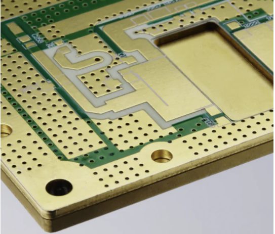
When designing RF and microwave circuits, selecting the right high frequency PCB laminates is critical to achieving optimal performance. These materials differ significantly in terms of dielectric properties, signal loss, manufacturability, and cost. The table below highlights some of the most widely used high frequency PCB laminates, comparing key technical specifications and their typical applications.
Each of these high frequency PCB laminates offers distinct advantages based on the application. Rogers materials, for example, are known for their stable Dk and easy fabrication, while PTFE-based laminates deliver the lowest possible signal loss at the cost of more complex processing. Taconic and F4B/F4BM series offer balanced performance and affordability, making them suitable for many commercial and industrial RF designs.
Choosing the right high frequency PCB laminates involves understanding these material trade-offs and aligning them with your performance, budget, and manufacturing needs.
Frequency Limitations of FR4: Why High Frequency PCB Laminates Are Necessary
While FR4 remains the most commonly used material in PCB manufacturing due to its low cost and ease of processing, it has clear limitations when used in high-frequency applications. Standard FR4 has a dielectric constant (Dk) of approximately 4.5 and a dissipation factor (Df) around 0.02. These properties may be acceptable for low-speed digital or analog circuits but become problematic at higher frequencies.
In real-world applications, the practical upper frequency limit of FR4 is around 1 GHz to 2.5 GHz. Beyond this range, the material begins to exhibit significant signal degradation. This is where high frequency PCB laminates offer a superior alternative. Compared to FR4, high frequency PCB laminates maintain a much lower and more stable Df, resulting in minimal signal attenuation and higher signal integrity.
FR4’s relatively high insertion loss leads to reduced transmission efficiency, especially over longer traces. Additionally, its unstable dielectric constant can cause impedance mismatches, reflections, and signal integrity issues—major concerns in RF, microwave, and 5G designs. In contrast, high frequency PCB laminates are engineered to provide predictable and reliable performance, even as frequencies climb into the multi-gigahertz or millimeter-wave range. As a result, designers working in advanced communication systems increasingly rely on high frequency PCB laminates to overcome the technical limits of FR4.
How to Choose the Right High Frequency Laminate: Key Criteria for High Frequency PCB Laminates
Selecting the appropriate high frequency PCB laminates is critical to ensuring signal integrity, thermal reliability, and manufacturability in RF and microwave designs. With many materials available on the market, understanding how to evaluate and match a laminate’s properties to your design requirements can significantly improve overall PCB performance.
Key Selection Criteria
-
Dk (Dielectric Constant):
The dielectric constant directly affects the impedance of transmission lines. A consistent and tightly controlled Dk is essential for maintaining predictable impedance across the board. Lower Dk values are often preferred in high-frequency applications to reduce signal delay and crosstalk. High-end high frequency PCB laminates offer stable Dk values across a wide temperature and frequency range.
-
Df (Dissipation Factor):
The dissipation factor measures dielectric loss, which contributes to signal attenuation. Materials with a low Df (e.g., <0.003) are ideal for minimizing signal loss, especially at frequencies above 1 GHz. This makes advanced PCB materials far superior to standard FR4, which typically has a much higher Df (~0.02).
-
CTE (Coefficient of Thermal Expansion):
A low and consistent CTE is crucial in multilayer designs to prevent layer misalignment or via cracking during thermal cycling. Advanced laminates generally offer better thermal stability, especially in complex RF stack-ups.
-
Compatibility with FR4 in Hybrid Stack-Ups:
In cost-sensitive designs, combining RF-grade materials with FR4 layers (hybrid stack-up) can be an effective strategy. However, this requires careful matching of CTE and process compatibility to avoid delamination or warping during fabrication.
Design Considerations
-
Controlled Impedance Routing:
Trace width, spacing, and dielectric thickness must be precisely tuned to match the target impedance, typically 50Ω or 100Ω differential. This is only achievable when using high frequency PCB laminates with stable dielectric properties.
-
Layer Stack-Up Design:
Strategic placement of signal, ground, and power planes helps isolate noise, reduce EMI, and maintain consistent impedance. High-frequency stack-ups often use thinner dielectrics and multiple ground layers.
-
Via and Grounding Strategies:
Proper via placement and grounding are essential to ensure clean return paths and suppress signal reflections. Techniques such as via stitching and ground pours further improve high-frequency performance in advanced PCB designs.
Choosing the right materials not only ensures functional reliability but also enables your design to meet strict performance benchmarks in today’s RF, 5G, and high-speed applications.
Best Design Practices for High Frequency PCBs Using High Frequency PCB Laminates
To fully harness the performance potential of high frequency PCB laminates, engineers must apply specific layout and stack-up strategies tailored to high-frequency signal behavior. Proper design practices not only reduce losses and EMI but also ensure your PCB performs reliably at GHz-level frequencies.
Routing Strategies
Efficient routing is essential when working with high frequency PCB laminates. High-frequency signals are highly sensitive to trace geometry and path discontinuities. Follow these best practices:
-
Keep traces short and direct to reduce propagation delay and signal loss.
-
Avoid 90° trace bends, which can cause impedance discontinuities and signal reflections. Use 45° angles or curved traces instead.
-
Match trace lengths in differential pairs to maintain signal timing and reduce skew, especially in RF and high-speed digital lines.
-
Maintain consistent trace width to preserve controlled impedance, which is supported by the uniform Dk properties of high frequency PCB laminates.
Power and Ground Layer Design
The power and ground plane configuration is a key factor in high-frequency PCB performance. With the help of high frequency PCB laminates, you can maintain signal integrity and suppress EMI:
-
Minimize return path loops by placing solid ground planes directly beneath signal layers, ensuring that high-frequency currents have a low-inductance return path.
-
Use ground stitching vias to tie together ground planes and improve shielding, especially around high-frequency components and transmission lines.
-
Decoupling capacitors should be placed as close as possible to IC power pins to reduce noise.
Sample Stack-Ups
When using high frequency PCB laminates, your layer stack-up design must account for both signal integrity and manufacturability. Below are typical configurations:
-
2-Layer Stack-Up
-
Top Layer: Signal + Components
-
Bottom Layer: Ground Plane
-
Use high frequency PCB laminates on both sides for RF trace stability.
-
4-Layer Stack-Up
-
6-Layer Stack-Up
By following these design practices and choosing the right materials, you can create PCBs that meet the stringent requirements of RF, 5G, satellite, and automotive applications.
Rigid-Flex in High Frequency PCB Applications Using High Frequency PCB Laminates
As electronics continue to evolve toward compact, lightweight, and high-performance systems, rigid-flex technology is becoming increasingly important—especially in high-frequency domains. When combined with high frequency PCB laminates, rigid-flex designs enable seamless integration of signal integrity, mechanical reliability, and space efficiency.
Use Cases
Rigid-flex PCBs with high frequency PCB laminates are widely used in advanced applications where flexibility and RF performance must coexist:
-
Wearable Devices: Medical monitors, smartwatches, and fitness trackers benefit from flexible RF circuits that can conform to the body while maintaining reliable wireless connectivity.
-
Aerospace Systems: Avionics, radar modules, and satellite communication units leverage rigid-flex designs for weight savings and durability, while relying on high frequency PCB laminates to handle GHz-level signal transmission.
-
mmWave Sensors: Automotive radar and industrial IoT devices often combine rigid signal processing sections with flexible sensor arms, demanding both physical flexibility and low-loss signal integrity.
Challenges and Material Compatibility
Integrating high frequency PCB laminates into rigid-flex constructions introduces several challenges:
-
Material Compatibility: Flex substrates (like polyimide) have very different mechanical and thermal properties compared to rigid materials like PTFE or Rogers. Balancing these differences requires careful laminate selection and process control.
-
Bend Reliability: High-performance RF materials tend to be more brittle than traditional flex materials. Designers must avoid placing sensitive RF layers in dynamic bending regions.
Hybrid Stack-Up Tips
To ensure performance and manufacturability, follow these stack-up guidelines when combining flex and rigid sections:
-
Use rigid materials like RO4000 or Taconic in the RF zones, while maintaining traditional flex materials in the bendable areas.
-
Design controlled impedance layers only in the rigid sections where precise Dk and Df values can be maintained.
-
Add shield layers around the flex sections to reduce EMI and signal coupling between RF and low-speed control lines.
-
Apply staggered via placement and keep critical high-frequency routing in the rigid zones to prevent bending stress on delicate RF traces.
When properly designed, rigid-flex PCBs using high frequency PCB laminates can deliver high-speed performance and mechanical versatility for cutting-edge technologies in aerospace, healthcare, and mmWave communications.
Are LED PCBs Considered High Frequency? Understanding the Role of High Frequency PCB Laminates
Most LED PCBs are not typically categorized as high-frequency designs. These PCBs are primarily used to drive LED arrays for lighting, displays, and indicator purposes, where the focus is on managing current and heat dissipation rather than high-speed signal transmission. The operating frequencies of standard LED circuits typically fall well below the GHz range, making them distinct from traditional high-frequency PCB applications.
Clarification: Most LED PCBs Are Not High-Frequency
LED PCBs generally operate at low frequencies in the range of 50 Hz to several kHz, particularly in applications involving power regulation and current control. In these circuits, the primary concerns are heat management, efficient power delivery, and ensuring uniform light output. These designs rarely require the precise dielectric properties and low-loss characteristics that are necessary for high-frequency signal transmission.
These PCBs may still use high frequency PCB laminates in certain applications that require enhanced thermal conductivity or reliability, but this does not typically categorize the entire LED industry under “high-frequency.”
Exceptions: Visible Light Communication (VLC) and High-Speed LED Drivers
Despite most LED PCBs operating at low frequencies, there are exceptions where high frequency PCB laminates become relevant:
-
Visible Light Communication (VLC): In VLC systems, LEDs are modulated at high frequencies (up to several MHz or more) to transmit data using visible light. These systems require high-speed signal integrity, and thus, the use of high frequency PCB laminates is necessary to support the high-frequency switching and communication protocols involved.
-
High-Speed LED Drivers: Some high-performance LED drivers, particularly those used in applications like high-end displays, automotive lighting, or advanced medical equipment, may require fast signal processing capabilities to ensure precise control of LED brightness and color. These drivers operate at much higher frequencies, necessitating specialized materials to minimize signal loss, maintain impedance control, and ensure optimal performance.
Most LED PCBs aren’t high-frequency, but applications like VLC and high-speed LED drivers need advanced materials for fast, precise signal control.
PCB Manufacturers & Material Suppliers to Know for High Frequency PCB Laminates
Selecting the right PCB manufacturer and material supplier is key to ensuring quality, reliability, and performance in high-frequency designs. Experienced providers understand the complex needs of such circuits and can assist with material selection, design, and fabrication.
Recommended PCB Manufacturers
Several PCB manufacturers are well-versed in producing high-performance boards using high frequency PCB laminates. They have the expertise to handle the unique challenges posed by high-frequency signals, such as impedance control, signal loss, and multi-layer construction.
-
PCBWay: Known for its extensive experience in both prototyping and mass production, PCBWay offers a range of capabilities for high-frequency PCBs, including controlled impedance routing and multilayer designs.
-
RushPCB: Specializing in quick-turn and high-frequency PCB fabrication, RushPCB provides high-quality materials and delivers rapid prototyping for RF, microwave, and other high-speed designs.
-
MadPCB: Focused on high-precision PCB manufacturing, MadPCB works with advanced materials and offers services that support complex RF and microwave designs.
-
Hemeixin PCB: A leading PCB manufacturer in China, Hemeixin offers cost-effective high-frequency PCB solutions using specialized materials for a range of industries, including telecommunications and automotive.
Leading Laminate Suppliers
Choosing the right high frequency PCB laminates is vital to achieving optimal performance. The following suppliers are known for providing top-tier materials that meet the demanding specifications of high-frequency applications:
-
Rogers Corporation: A leader in advanced PCB materials, Rogers offers a variety of high-performance laminates like the RO4000 and RT/duroid series. These materials are designed for stable performance in high-frequency environments and are widely used in RF, microwave, and millimeter-wave applications.
-
DuPont: Known for its high-quality materials, DuPont offers products such as the Pyralux series, which are ideal for high-performance applications requiring low loss and reliable signal integrity.
-
Taconic: Specializing in both flexible and rigid laminates, Taconic provides materials that offer excellent low-loss performance and are widely used in high-speed and microwave circuit designs.
-
Bicheng PCB: Offering cost-effective solutions, Bicheng PCB provides high-performance materials that are perfect for moderate RF and microwave applications.
Things to Look For
When selecting PCB manufacturers and laminate suppliers for high-frequency designs, consider the following critical factors:
-
Impedance Control Capabilities: High-frequency designs require tight control over impedance to ensure signal integrity. Look for manufacturers with experience in designing and producing PCBs with precise impedance control, particularly for RF and microwave applications.
-
Multi-Layer RF Board Experience: High-frequency applications often require multi-layer PCBs to isolate signals and minimize interference. Choose manufacturers with a proven track record of handling complex, multi-layer RF boards.
-
Material Certifications (UL, IPC, etc.): Ensure that both the manufacturer and the laminate supplier hold relevant industry certifications like UL and IPC, which guarantee that the materials and manufacturing processes meet high standards for quality, reliability, and safety.
By choosing the right manufacturers and suppliers, you can ensure the successful production of high-quality materials, optimized for your specific design needs in RF, microwave, and other high-speed applications.
FQAs Abut High Frequency PCB Laminates
What is the best PCB material for high frequency?
The best PCB materials for high-frequency applications are those with low dielectric loss (Df) and stable dielectric constant (Dk). Some of the top choices include materials like Rogers RO4000 series, RT/duroid® series, Taconic TLY and PTFE (Teflon). These materials are specially designed to maintain signal integrity and reduce loss at high frequencies, making them ideal for RF, microwave, and millimeter-wave circuits.
What are high frequency laminates?
High-frequency laminates are specialized PCB materials used for circuits operating at frequencies above 500 MHz, typically in the GHz range. These laminates are engineered to have low dielectric loss (Df) and stable dielectric constant (Dk) to ensure minimal signal degradation. Common high-frequency laminates include materials such as Rogers RO4000, RT/duroid, and PTFE, which provide excellent performance in RF, microwave, and high-speed digital applications.
What is the highest frequency for FR4?
FR4, the most common PCB material, has limitations when it comes to high-frequency applications. Its highest practical frequency range is typically between 1 GHz to 2.5 GHz. Beyond this range, FR4’s dielectric properties—particularly its higher dissipation factor (Df) and less stable dielectric constant (Dk)—cause significant signal loss and impedance instability, making it unsuitable for higher-frequency designs. For frequencies above 2.5 GHz, alternative materials like Rogers or PTFE are recommended.
What are high frequency PCBs?
High-frequency PCBs are printed circuit boards designed to operate at frequencies above 500 MHz, often extending into the GHz range. These PCBs are used in applications like RF communication, microwave circuits, 5G antennas, satellite systems, and radar. To meet the demands of these high-frequency signals, these PCBs are made from specialized laminates that offer low dielectric loss, stable impedance, and minimal signal degradation, ensuring reliable performance at high speeds.