
Materials in High Frequency PCB Communication Circuits
High-frequency PCBs (Printed Circuit Boards) are specialized circuit boards designed to operate at frequencies typically above 1 GHz, built with materials and techniques that minimize signal loss, interference, and distortion. These boards are characterized by low dielectric loss, excellent signal integrity, and precise impedance control, making them essential for high-speed, high-performance applications. In modern communication technologies, high-frequency PCBs play a critical role in supporting fast, reliable data transmission. They are integral to wireless communication, satellite systems, radar, and 5G networks, where maintaining signal quality is crucial. High-frequency PCB communication circuits are vital in ensuring these systems operate efficiently, as even slight signal degradation can lead to performance issues. Therefore, the design and manufacture of high-frequency PCBs are essential for achieving the high data rates and low latency required in today’s advanced communication networks.
Basic Concepts of High-Frequency PCB Communication Circuits
High-frequency PCBs are specialized printed circuit boards designed to handle signals operating at frequencies above 1GHz. These PCBs are essential for applications requiring high-speed data transmission, such as wireless communication, radar, and satellite systems. Unlike standard PCBs, high-frequency PCBs are built using specific materials and design techniques that ensure the integrity of high-frequency signals. The increased demand for data-intensive communication technologies, such as 5G and IoT, has made high-frequency PCB communication circuits a fundamental part of modern electronics.
The key difference between high-frequency PCBs and standard PCBs lies in their design and materials. While standard PCBs are designed for lower frequency ranges (typically under 1GHz), high-frequency PCBs are optimized to minimize signal loss, reflection, and noise. High-frequency PCBs often use advanced materials like PTFE (Polytetrafluoroethylene), ceramics, or low-loss epoxy laminates, which are capable of maintaining signal integrity at high frequencies. In contrast, standard PCBs typically use FR4, a material that is not ideal for high-frequency applications due to higher signal attenuation.
The primary features of high-frequency PCBs include low loss, high signal integrity, and fast signal transmission. These characteristics are critical for high-frequency PCB communication circuits, as even minor losses can severely degrade performance. Low loss materials and precise impedance matching are essential to ensure that signals are transmitted with minimal interference or distortion. Additionally, maintaining high signal integrity is crucial for preventing errors or data corruption, especially in high-speed communication applications. Fast signal transmission ensures that data can be sent and received with minimal latency, which is vital in communication circuits that require real-time processing.
Material Selection for High-Frequency PCB Communication Circuits
Material selection is a critical factor in the performance of high-frequency PCBs, especially for high-frequency PCB communication circuits. The choice of material directly impacts the signal integrity, loss, and overall functionality of the PCB. High-frequency PCBs are typically constructed using advanced materials that are engineered to minimize signal attenuation, maintain low dielectric loss, and provide stable performance at high frequencies. Below are some of the most commonly used materials for high-frequency PCBs:
-
PTFE (Polytetrafluoroethylene):
PTFE, commonly known by the brand name Teflon, is one of the most popular materials for high-frequency PCBs. It has an extremely low dielectric constant and low loss tangent, making it ideal for high-frequency applications where signal integrity is crucial. PTFE is commonly used in applications such as radar, satellite communication, and wireless communication circuits. Its excellent electrical properties enable high-speed data transmission with minimal signal degradation, which is essential for high-frequency PCB communication circuits. -
Ceramics:
Ceramic materials are another popular choice for high-frequency PCBs. Ceramics have superior dielectric properties, which allow them to perform well in high-frequency environments. Ceramic-based PCBs are known for their low signal loss, high thermal conductivity, and stability in extreme conditions. These properties make them ideal for applications in RF (Radio Frequency) and microwave communication systems, aerospace, and military applications, where high reliability and precision are required. The use of ceramic materials is particularly beneficial in situations where durability and performance at elevated frequencies are key. -
FR4 (Flame-Retardant 4):
While FR4 is commonly used in standard PCBs, it is also used in some high-frequency applications. However, its properties are not as suited for high-frequency use as materials like PTFE or ceramics. FR4 has a higher dielectric loss and higher signal attenuation compared to materials like PTFE, making it less ideal for high-frequency PCB communication circuits. Nevertheless, FR4 is still widely used for low-to-medium-frequency applications, especially where cost is a significant consideration. In high-frequency PCBs, FR4 is often used as a substrate in multi-layer boards, where its performance can be compensated for with other materials. -
LCP (Liquid Crystal Polymer):
LCP is another material used in high-frequency PCBs, particularly when very low loss is required. LCP has a very stable dielectric constant and low dissipation factor, making it suitable for high-frequency communication circuits. Its ability to maintain signal integrity and minimize loss at high frequencies makes it a good choice for applications in telecommunications, automotive radar, and other high-speed communication systems.
Properties and Applications of Each Material
-
PTFE is primarily used for very high-frequency applications due to its low dielectric constant (usually between 2.0 and 2.5) and very low loss tangent. It is ideal for high-frequency PCB communication circuits in radar systems, satellite communication, and 5G networks.
-
Ceramics offer excellent dielectric stability, thermal conductivity, and low loss, making them the material of choice for high-frequency applications in aerospace, defense, and microwave communication systems. Their ability to operate in extreme environments also contributes to their popularity in high-reliability applications.
-
FR4 remains the go-to material for lower-frequency applications in many consumer electronics, though it is often supplemented with higher-performance materials in multi-layer PCBs. In high-frequency applications, it is typically used for boards where signal performance demands are not extreme, and cost efficiency is a consideration.
-
LCP is often used in advanced communication systems such as cellular base stations, automotive radar, and high-frequency testing equipment, where low signal loss and high data rate transmission are necessary.
The Importance of Material Selection in High-Frequency Communication Circuits
Material selection plays an essential role in the performance of high-frequency PCB communication circuits. The materials used in high-frequency PCBs must have excellent electrical properties to ensure that signals can be transmitted without significant loss or distortion. Poor material choices can result in signal attenuation, reflection, crosstalk, and electromagnetic interference (EMI), all of which can degrade the overall performance of communication systems.
Materials with low dielectric loss and stable properties at high frequencies are necessary to ensure that high-frequency signals maintain their integrity over long distances or through complex circuit paths. For instance, using PTFE or ceramics ensures minimal signal degradation, while materials like FR4 may require additional design considerations (such as impedance matching and signal routing) to perform effectively in high-frequency applications.
In high-frequency PCB communication circuits, the right material helps in achieving faster data transmission rates, reduced signal distortion, and improved overall system reliability. Therefore, selecting the appropriate material is not just about cost but about ensuring the long-term success and performance of the communication system.
Challenges in High-Frequency PCB Communication Circuits Design
Designing high-frequency PCBs presents unique challenges that require specialized knowledge and techniques to ensure optimal performance. These challenges are particularly pronounced in high-frequency PCB communication circuits, where the quality of signal transmission is critical. Even small errors or oversights in design can lead to significant performance degradation, making it essential to address issues related to signal integrity, transmission line design, electromagnetic interference (EMI), and noise management. Below are some of the key challenges faced in high-frequency PCB design:
Signal Integrity Issues: Reflection, Crosstalk, Signal Attenuation
Signal integrity is one of the most critical aspects of high-frequency PCB communication circuits. When high-frequency signals travel through traces on a PCB, they can experience various forms of degradation that negatively affect the overall performance of the system.
-
Reflection: Reflection occurs when a signal encounters an impedance mismatch along the transmission line, causing part of the signal to reflect back toward the source. This can lead to signal distortion and data errors, which are especially problematic in high-frequency applications. Ensuring that the impedance of traces and components is correctly matched is vital to minimizing reflections.
-
Crosstalk: Crosstalk happens when signals from one trace or circuit interfere with signals in another nearby trace. At high frequencies, the electromagnetic field of one signal can couple into an adjacent signal, causing unwanted interference. In high-frequency PCB communication circuits, managing crosstalk is crucial to prevent errors in data transmission, especially when signals are traveling at very fast rates.
-
Signal Attenuation: Signal attenuation refers to the gradual loss of signal strength as it travels through the PCB traces. At high frequencies, attenuation becomes a significant issue, as the signal’s energy dissipates quickly, leading to weaker signals at the receiving end. Using materials with low dielectric loss and ensuring proper trace widths and lengths can help minimize this effect.
Transmission Line Design: Impedance Matching
One of the primary challenges in high-frequency PCB design is ensuring proper impedance matching across the entire signal path. In high-frequency PCB communication circuits, any deviation in the characteristic impedance of the transmission lines can result in signal reflections, distortions, and data loss.
-
Impedance Matching: The impedance of a PCB trace must match the impedance of the source and load (such as connectors, ICs, and other components) to prevent reflections. Mismatched impedance causes the signal to reflect back toward the source, resulting in signal degradation and potential data errors. This is especially important when dealing with high-speed signals in communication circuits, as even small mismatches can significantly impact performance.
-
Trace Geometry: Achieving impedance matching often requires careful design of the trace geometry, such as the width of the trace and the distance between the trace and the ground plane. For example, microstrip lines (traces on the surface of the PCB) and stripline designs (traces sandwiched between layers) need to be precisely designed to maintain consistent impedance.
Electromagnetic Interference (EMI) and Electromagnetic Compatibility (EMC) Issues
EMI and EMC are major concerns in high-frequency PCB design, particularly in high-frequency PCB communication circuits where fast signals can easily radiate or interfere with nearby components.
-
Electromagnetic Interference (EMI): High-frequency signals can emit electromagnetic radiation that can interfere with other circuits and systems. EMI can affect nearby electronics, degrade performance, and cause malfunction. The higher the frequency of the signals, the more pronounced the EMI issues can be. Effective shielding, proper routing, and ground plane management are essential for minimizing EMI.
-
Electromagnetic Compatibility (EMC): EMC refers to the ability of a system to operate without causing interference to other systems or being susceptible to external interference. In high-frequency PCB communication circuits, ensuring EMC involves designing the PCB layout to reduce emissions, improve noise filtering, and prevent external sources of interference from affecting the circuit’s performance.
Ground Plane and Power Noise Management
In high-frequency PCB communication circuits, managing ground plane and power noise is crucial to ensuring stable signal transmission and minimizing noise-related issues.
-
Ground Plane Integrity: The ground plane serves as the reference point for all signals and is critical for reducing noise and maintaining stable performance. If the ground plane is poorly designed or has large gaps, it can lead to issues like voltage fluctuations, EMI, and signal integrity problems. For high-frequency circuits, ensuring that the ground plane is continuous and free from interruptions is vital to maintain consistent signal behavior.
-
Power Noise: High-frequency circuits are sensitive to power supply noise, as fluctuations in voltage or current can introduce noise into the signal path. Power integrity issues, such as voltage spikes or ripple, can degrade signal quality and disrupt the performance of high-frequency communication circuits. Implementing decoupling capacitors and proper power distribution techniques can help reduce power noise and stabilize the power supply.
The challenges in designing high-frequency PCB communication circuits are multifaceted, and addressing them requires a comprehensive understanding of signal integrity, impedance matching, EMI/EMC issues, and noise management. Designers must carefully consider all of these factors during the planning, design, and manufacturing stages to ensure that the final PCB performs reliably in high-frequency communication systems. Ensuring the integrity of signals, minimizing interference, and maintaining a stable power supply are essential to achieving optimal performance in modern high-speed communication applications.
Key Techniques in High-Frequency PCB Communication Circuits Design
Designing high-frequency PCB communication circuits requires the application of specialized techniques that ensure the integrity and performance of the signal throughout the PCB. The key techniques in high-frequency PCB design focus on maintaining signal quality, minimizing interference, and optimizing the circuit layout for the high-speed transmission of data. Here are some essential techniques used in the design of high-frequency PCBs:
Impedance Matching and Microstrip Design: How to Maintain Signal Integrity with Microstrip or Stripline Designs
Impedance matching is critical in high-frequency PCB communication circuits, as any mismatch in impedance can lead to signal reflections, loss of data integrity, and performance degradation. Microstrip and stripline designs are commonly used to ensure that signals maintain their integrity over long distances.
-
Microstrip Design: A microstrip is a type of transmission line where the signal trace is placed on the surface of the PCB, with a ground plane beneath it. The design of the trace width and the spacing between the trace and the ground plane directly affects the characteristic impedance of the transmission line. Typically, a 50-ohm impedance is desired for RF (radio frequency) applications, and the trace width must be calculated to maintain this impedance. Careful design of the microstrip ensures that signals do not suffer from reflection or attenuation as they travel along the PCB.
-
Stripline Design: In a stripline configuration, the signal trace is sandwiched between two ground planes, which provides better isolation and reduced noise compared to microstrip lines. While stripline designs are more complex and may require more layers in the PCB stack-up, they offer superior signal integrity, especially at higher frequencies. This makes stripline an ideal choice for high-frequency PCB communication circuits in more demanding applications such as radar or satellite systems.
Impedance matching ensures that the signal travels without degradation, providing stable and reliable data transmission in high-speed communication systems.
Choosing the Right Stack-Up Structure: Use of Multi-Layer PCBs
The stack-up structure of a PCB refers to the arrangement of layers used in the board’s construction, which is especially important in high-frequency PCB communication circuits. Multi-layer PCBs are often required for high-frequency designs, as they allow for better control over impedance, noise, and signal paths.
-
Multi-Layer PCBs: Using a multi-layer design allows for optimal routing of high-frequency signals and the placement of dedicated ground and power planes. These layers help minimize crosstalk, reduce noise, and enhance signal integrity by providing better isolation for high-frequency traces. A proper multi-layer stack-up can also help manage the return currents of high-speed signals, which is crucial for maintaining stable signal transmission.
-
Optimizing Layer Placement: The placement of signal, ground, and power layers is essential for high-frequency PCBs. For example, placing the ground plane close to the signal traces helps reduce the loop area of the return path, which minimizes noise and improves signal integrity. Additionally, the arrangement of layers should minimize signal cross-talk and interference, which can be particularly problematic in high-frequency PCB communication circuits.
Via and Blind Via Design: Optimizing Signal Paths Through Vias
Vias are essential components in multi-layer PCBs, allowing signals to pass from one layer to another. However, in high-frequency PCB communication circuits, vias can introduce problems such as signal loss, increased inductance, and impedance discontinuities if not properly designed.
-
Via Design Considerations: Vias should be designed with minimal size and inductance to reduce the potential for signal degradation. For high-frequency applications, the use of blind vias (vias that do not go all the way through the PCB) is often preferred, as they reduce the path length and inductance. Micro-vias are also commonly used in high-frequency designs due to their small size and ability to minimize signal losses.
-
Via Stub Reduction: Long via stubs (unconnected portions of the via) can cause reflections and signal degradation. These stubs should be minimized or eliminated to ensure that high-frequency signals pass through the vias smoothly without interference. For high-frequency PCB communication circuits, optimizing the via design can significantly improve the overall performance of the PCB.
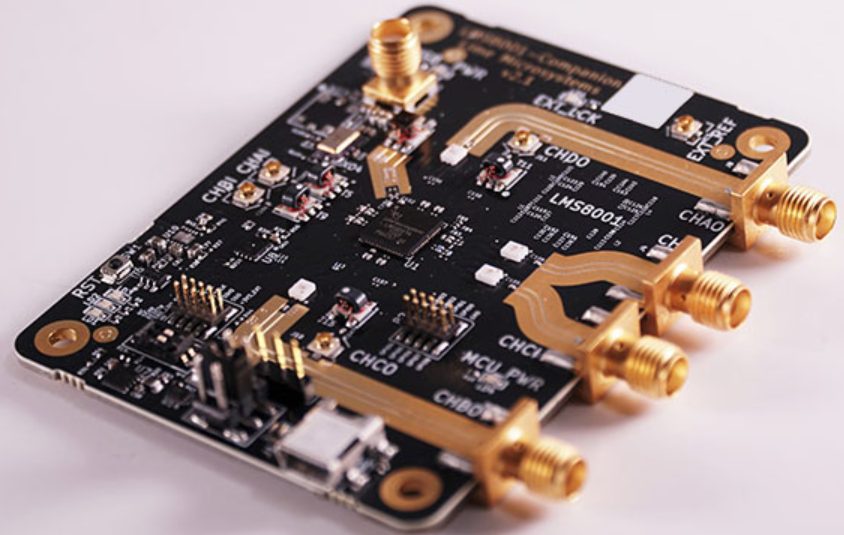
High-Frequency Connectors and Interconnects: Choosing Suitable Connectors for High-Frequency Signals
Choosing the appropriate connectors and interconnects is crucial for maintaining signal integrity in high-frequency PCB communication circuits. Connectors are often the weakest link in a high-frequency system, and their performance can significantly impact the overall circuit performance.
-
Connector Types: Connectors used in high-frequency applications should have low insertion loss, high return loss, and minimal signal reflection. RF connectors such as SMA (SubMiniature version A), SMB, and BNC connectors are designed specifically for high-frequency signals and provide the necessary performance to maintain signal quality. Choosing connectors with appropriate impedance (typically 50 ohms for most RF applications) is also essential for preventing impedance mismatches.
-
Interconnect Design: The layout of the PCB should be optimized to ensure that the connector’s signal path is as short and direct as possible to minimize signal loss and delay. Poorly designed interconnects can introduce significant signal degradation and interference, especially at high frequencies. For high-frequency PCB communication circuits, minimizing the length of the transmission lines leading to connectors helps maintain optimal signal integrity.
Thermal Management: Preventing Heat from Affecting Circuit Performance
Effective thermal management is a significant challenge in high-frequency PCB communication circuits, especially as the speed and density of components increase. High-frequency circuits generate heat, and excessive heat can degrade performance, damage components, and lead to circuit failure.
-
Heat Dissipation: High-frequency signals can cause certain components, especially high-power components, to generate heat. To prevent this, proper heat dissipation techniques should be employed, such as using heat sinks, thermal vias, or dedicated heat-spreading materials. Ensuring a low thermal resistance path for heat to escape from the PCB helps keep temperatures within safe operating limits.
-
Temperature Control: Monitoring and managing temperature variations in high-frequency PCB communication circuits is crucial to maintaining signal integrity. Excessive heat can cause dielectric materials to break down, leading to increased losses and reduced performance. For this reason, designers often integrate temperature sensors into high-frequency PCBs to monitor thermal conditions and ensure reliable operation.
Implementing these key techniques in high-frequency PCB communication circuits design is essential for maintaining signal integrity, ensuring optimal performance, and minimizing potential failures in high-speed communication systems. By focusing on impedance matching, proper stack-up structures, optimized via designs, high-quality connectors, and effective thermal management, designers can build robust and reliable PCBs that perform efficiently even at high frequencies. These techniques, when executed correctly, provide the foundation for high-performance communication circuits that meet the stringent demands of modern technology.
Applications of High-Frequency PCB Communication Circuits
High-frequency PCB communication circuits are pivotal in a wide range of modern communication technologies. These circuits are designed to handle the demands of high-speed signal processing, ensuring minimal signal degradation and optimal performance. Below are some of the most prominent applications where high-frequency PCB communication circuits are integral to achieving reliable and high-performance communication systems:
Wireless Communication and High-Frequency PCB Communication Circuits
Wireless communication systems rely heavily on high-frequency PCB communication circuits to transmit and receive signals at high speeds. These systems operate in the radio frequency (RF) spectrum, where signals typically range from a few GHz to tens of GHz.
-
Wi-Fi and Bluetooth: Both Wi-Fi and Bluetooth use high-frequency PCB communication circuits to support high-speed data transmission. Wi-Fi systems, especially those operating on 5 GHz and 6 GHz bands, require high-frequency PCBs to minimize signal loss and interference. Similarly, Bluetooth, especially with the increasing adoption of Bluetooth 5.0 and beyond, needs precise PCB design to ensure minimal data loss and reliable connectivity.
-
LTE and 5G Networks: The evolution of mobile networks, from LTE to 5G, has placed increased demands on high-frequency PCB communication circuits. 5G, for instance, operates at much higher frequencies (up to 100 GHz in some cases), requiring sophisticated designs to handle massive amounts of data at very high speeds. These high-frequency PCBs are crucial for achieving low latency, high data throughput, and stable connections in 5G base stations, mobile devices, and small cells.
The performance of wireless communication devices depends on high-frequency PCBs to maintain signal integrity and reduce interference in crowded and noisy environments.
Radar and Satellite Communication with High-Frequency PCB Communication Circuits
Radar and satellite communication systems are integral to applications such as weather monitoring, air traffic control, military defense, and navigation. These systems rely on high-frequency PCB communication circuits to process signals with extremely high precision.
-
Radar Systems: Radar systems, which operate in the microwave frequency range (typically from 1 GHz to 100 GHz), rely on high-frequency PCBs for signal transmission, reception, and processing. The main challenge in radar PCB design is managing signal reflection, interference, and attenuation, especially at higher frequencies. High-frequency PCB communication circuits are designed to minimize these issues through advanced impedance matching and careful trace routing.
-
Satellite Communication: Satellite communication systems also require high-frequency PCB communication circuits due to the need for precise signal transmission across long distances. These systems often operate in the C-band, Ku-band, or Ka-band (from 4 GHz to 30 GHz), and the high-frequency PCBs help ensure that signals are transmitted with minimal loss. In these systems, high-frequency PCB designs must also account for factors like signal distortion and Doppler shifts due to the movement of satellites.
Both radar and satellite systems benefit from high-frequency PCBs that ensure signals remain strong, clear, and accurate, allowing for high-performance operation in critical applications.
Fiber Optic Communication and High-Frequency PCB Communication Circuits
Fiber optic communication systems are known for their ability to transmit data at incredibly high speeds over long distances. While fiber optics themselves are used for the physical transmission of light signals, high-frequency PCB communication circuits are still essential in the electronic components that support fiber optic systems.
-
Optical Transceivers and Modulators: In fiber optic communication, high-frequency PCB communication circuits are crucial for the design of optical transceivers, which convert electrical signals into optical signals and vice versa. These transceivers must operate at speeds of 10 Gbps, 40 Gbps, or even 100 Gbps, requiring high-frequency PCBs that can handle these fast signals without causing data loss or distortion.
-
Signal Processing: Signal processing circuits that interface with fiber optic systems, such as amplifiers, modulators, and demodulators, also rely on high-frequency PCBs to ensure the high-speed, low-loss transmission of data. High-frequency PCB communication circuits are critical in ensuring that these devices operate with high efficiency and minimal error rates.
Fiber optic systems used in telecommunications, data centers, and high-speed internet applications all rely on high-frequency PCB communication circuits to achieve the necessary performance for ultra-fast data transmission.
Broadcast and Television Communication Using High-Frequency PCB Communication Circuits
Broadcast and television communication systems use high-frequency PCB communication circuits to ensure high-quality video and audio signal transmission. These systems require precision in signal processing to maintain clarity and consistency, whether for live broadcasts or recorded content.
-
Broadcast Transmitters and Receivers: Broadcast transmitters for television and radio often operate in the UHF (Ultra High Frequency) and VHF (Very High Frequency) bands, which can range from 30 MHz to 3 GHz. These transmitters rely on high-frequency PCB communication circuits to process signals for transmission over the airwaves.
-
Television Set-Top Boxes and Satellite Dishes: Set-top boxes, satellite receivers, and other broadcast-related equipment also rely on high-frequency PCB communication circuits to decode and display high-definition content. These devices require robust designs that can handle high-frequency signals with minimal noise and distortion.
The reliability of broadcast and television communication systems heavily depends on high-frequency PCB communication circuits that ensure accurate signal processing, minimal interference, and high-quality transmission of both video and audio.
Automotive Communication and High-Frequency PCB Communication Circuits
Modern vehicles rely increasingly on high-frequency PCB communication circuits to support a wide range of communication technologies for safety, navigation, and infotainment. These applications require fast and reliable data transfer to ensure the smooth operation of various automotive systems.
-
Vehicle-to-Everything (V2X) Communication: V2X communication is critical for enabling vehicles to communicate with each other, traffic signals, and infrastructure. This communication often operates in the 5.9 GHz band, requiring high-frequency PCB communication circuits to maintain low latency and high reliability for real-time traffic information and collision avoidance.
-
Radar and LiDAR for Autonomous Vehicles: Autonomous vehicles use radar and LiDAR systems to detect obstacles, monitor the surroundings, and navigate safely. These systems operate in the GHz frequency range and rely on high-frequency PCB communication circuits for precise signal processing. Radar and LiDAR sensors require high-frequency PCBs that can handle fast signal switching and ensure accurate data is relayed to the vehicle’s processing unit.
-
In-Car Infotainment Systems: Infotainment systems, including navigation, media streaming, and wireless connectivity, also rely on high-frequency PCB communication circuits for seamless data transmission. These systems use Wi-Fi, Bluetooth, and 4G/5G communication technologies to enable streaming and connectivity within the vehicle.
In the automotive sector, high-frequency PCB communication circuits are essential for enabling the smart features and safety systems that are increasingly standard in modern vehicles.
The applications of high-frequency PCBs span a wide array of industries, from wireless communication and radar systems to automotive and fiber optic communication. In each of these fields, these PCBs are vital for ensuring the reliable and efficient transmission of high-speed data, supporting the continued growth and evolution of advanced communication technologies. The performance of these systems relies heavily on well-designed circuits, which allow for fast, accurate, and interference-free communication across various platforms.
Manufacturing and Testing of High-Frequency PCB Communication Circuits
The manufacturing and testing of high-frequency PCB communication circuits involve specialized processes and equipment to ensure the final product meets the rigorous performance requirements for high-speed data transmission. These PCBs must be carefully constructed and thoroughly tested to meet the demanding standards of modern communication systems. Below is an overview of the challenges, solutions, and methods involved in the manufacturing and testing of high-frequency PCBs.
Manufacturing Processes for High-Frequency PCBs: Challenges and Solutions
The manufacturing of high-frequency PCB communication circuits presents unique challenges due to the need for precise control over materials, geometries, and manufacturing techniques. High-frequency circuits are sensitive to minor variations in design and manufacturing, and any small mistake can significantly impact performance. Here are some of the primary challenges and solutions in high-frequency PCB manufacturing:
-
Material Selection and Laminate Choices: High-frequency PCBs require materials with low dielectric loss and stable electrical properties at high frequencies. Traditional PCB materials like FR4 may not perform adequately in high-frequency applications. Instead, materials like PTFE (Polytetrafluoroethylene), ceramic-filled composites, and advanced resin systems are often used. Choosing the right material is essential for minimizing signal loss and maintaining integrity over long distances. These materials are more expensive and difficult to process, but they provide the necessary performance for high-frequency applications.
-
Precision in Trace Geometry: The traces in high-frequency PCBs need to be carefully designed to maintain specific impedance values and avoid signal degradation. This requires precise control over trace width, spacing, and layer stacking. A small variation can lead to impedance mismatches, signal reflection, or attenuation. Advanced manufacturing techniques such as laser etching and high-precision photolithography are often employed to achieve the required accuracy in trace geometry for high-frequency applications.
-
Multi-layer Design Complexity: High-frequency designs often require multi-layer PCBs to handle the routing of high-speed signals while maintaining signal integrity. Manufacturing multi-layer PCBs with tight tolerances for layer registration and alignment is more complex and requires specialized equipment. The layers must be accurately bonded and aligned to prevent issues such as signal degradation or crosstalk between layers. Careful design and manufacturing techniques are essential to achieve optimal performance in high-frequency applications.
-
Via Design and Hole Metallization: The use of vias in multi-layer PCBs introduces challenges in terms of signal integrity and impedance control. For high-frequency circuits, the vias need to be designed with minimal inductance and resistance to prevent signal losses. Techniques such as micro-via designs and blind vias are commonly used, but they require highly precise drilling and metallization processes to ensure reliability in high-frequency applications.
How to Test High-Frequency PCBs: Signal Transmission Testing, Distortion Analysis, EMI Testing, etc.
Testing high-frequency PCBs is essential to verify that they meet the performance standards for signal transmission, noise management, and electromagnetic compatibility (EMC). Various testing methods are used to ensure that the high-frequency PCB communication circuits function correctly in their intended applications:
-
Signal Transmission Testing: Signal integrity is one of the most critical factors in high-frequency PCB testing. Signal transmission testing involves sending signals through the PCB and measuring the results at various points along the signal path. This helps identify any issues related to attenuation, distortion, or reflections. Time-domain reflectometry (TDR) is often used to analyze signal transmission, pinpointing where impedance mismatches or signal losses may occur in the PCB.
-
Distortion Analysis: High-frequency signals are particularly susceptible to distortion, which can result in data errors or signal degradation. Distortion analysis helps identify issues such as phase shifts, non-linearities, and harmonic distortions that can occur in the PCB. Distortion can be caused by factors such as imperfect materials, poor PCB layout, or improper grounding. Using advanced tools like spectrum analyzers, designers can measure the degree of signal distortion and address the root causes in the PCB design.
-
EMI Testing: Electromagnetic interference (EMI) is a significant concern in high-frequency PCB communication circuits, as these circuits are prone to emitting or receiving unwanted signals that can interfere with nearby systems. EMI testing ensures that the PCB meets the required electromagnetic compatibility (EMC) standards. This involves measuring the electromagnetic radiation emitted by the PCB and comparing it to regulatory limits. Special chambers, such as anechoic chambers, are used for this testing, where the PCB is tested in an environment that isolates external signals. If the PCB exceeds the EMI limits, design changes such as adding shielding, optimizing ground planes, or using filtering components are implemented to reduce emissions.
-
Impedance and Crosstalk Testing: Ensuring that the impedance of traces is correctly matched and minimizing crosstalk between adjacent traces are key factors in high-frequency PCB communication circuits. Testing for impedance mismatch and crosstalk helps identify areas where signal integrity might be compromised. Specialized equipment like vector network analyzers (VNAs) is used to measure the impedance and transmission characteristics of the PCB.
High-Frequency PCB Testing Equipment: Network Analyzers, Oscilloscopes, etc.
High-frequency PCB testing requires specialized equipment to accurately assess the performance of high-frequency PCB communication circuits. Below are some of the most commonly used testing tools:
-
Network Analyzers (VNAs): Vector network analyzers are essential tools for testing the frequency response and impedance of high-frequency circuits. VNAs can measure parameters such as reflection and transmission coefficients (S-parameters) to analyze the integrity of signals traveling through the PCB. VNAs are used to evaluate the overall performance of high-frequency PCB communication circuits by assessing their impedance matching, attenuation, and phase response across a range of frequencies.
-
Oscilloscopes: Oscilloscopes are used to measure the waveform of signals at various points in the PCB. High-frequency oscilloscopes, capable of operating at GHz speeds, are required to accurately capture fast signals without introducing distortion. These instruments help analyze signal rise times, waveform distortion, and overall signal integrity, offering valuable insights into the behavior of communication circuits under real-world conditions.
-
Spectrum Analyzers: Spectrum analyzers are used to measure the power spectrum of signals and detect any unwanted frequency components, such as harmonics or spurious signals. These tools are particularly useful for EMI testing and ensuring that the high-frequency PCB communication circuits meet regulatory standards for electromagnetic emissions.
-
Time Domain Reflectometers (TDR): TDRs are used to evaluate the quality of signal traces by sending electrical pulses down the PCB’s signal paths and measuring the reflections that occur. The data from TDR testing can help identify areas of the PCB where impedance mismatches or poor connections are affecting signal quality.
The manufacturing and testing of high-frequency PCBs are critical to ensuring that these circuits operate reliably and efficiently in high-speed communication systems. The challenges in manufacturing, such as material selection, precision design, and multi-layer construction, must be addressed with specialized techniques and equipment. Testing, including signal transmission analysis, distortion testing, and EMI testing, ensures that the PCBs meet the stringent requirements for modern communication technologies. Utilizing the right testing equipment, such as network analyzers, oscilloscopes, and TDRs, enables designers to verify the performance of the PCB and make necessary adjustments to maintain signal integrity and overall performance.
Future Trends in High-Frequency PCB Communication Circuits
As the demand for faster and more reliable communication technologies continues to grow, high-frequency PCB communication circuits are becoming increasingly crucial in supporting next-generation systems. The rapid advancement of 5G technology, along with the emergence of quantum communication and other cutting-edge technologies, is driving innovations in the design and manufacturing of high-frequency PCBs. Here are some key trends shaping the future of these circuits:
Demand for High-Frequency PCBs with the Growth of 5G and Future Communication Technologies
The rollout of 5G networks is one of the most significant drivers of demand for high-frequency PCB communication circuits. 5G offers much faster data transmission speeds, lower latency, and more reliable connections compared to previous generations. To support these advancements, high-frequency PCBs must be capable of operating at much higher frequencies (up to 100 GHz and beyond), while maintaining low signal loss, high impedance matching, and minimal crosstalk.
-
5G Infrastructure: The demand for high-frequency PCB communication circuits is not only driven by consumer devices, such as smartphones and tablets, but also by the infrastructure needed to support 5G networks. Base stations, small cells, and antennas require high-frequency PCBs to handle the increased data throughput and faster signal processing speeds needed for 5G communication.
-
Beyond 5G (6G): Looking ahead, the transition from 5G to 6G will push high-frequency PCB communication circuits even further. 6G is expected to operate at frequencies above 100 GHz, bringing new challenges and opportunities for high-frequency PCB design. These ultra-high frequencies will require even more advanced materials, precise manufacturing, and optimized designs to ensure reliable performance.
As 5G and future communication technologies continue to evolve, high-frequency PCB communication circuits will be at the core of enabling the high-speed, high-capacity data transmission required by next-generation networks.
Emerging Materials for High-Frequency PCBs
As high-frequency PCB communication circuits operate at increasingly higher frequencies, the materials used in their construction must also evolve to maintain signal integrity and minimize losses. Traditional PCB materials like FR4 are no longer suitable for these high-speed applications, leading to the development of new, advanced materials.
-
PTFE (Polytetrafluoroethylene): PTFE is a popular choice for high-frequency PCBs due to its low dielectric loss and stable electrical properties at high frequencies. PTFE is ideal for applications like RF and microwave circuits, as it ensures minimal signal attenuation and maintains high signal integrity over long distances. However, PTFE can be more difficult to manufacture and more expensive than conventional PCB materials.
-
Ceramic-Based PCBs: Ceramic substrates, such as alumina and beryllia, are increasingly being used in high-frequency PCB communication circuits due to their high thermal conductivity and low signal loss at microwave frequencies. Ceramic-based PCBs are ideal for applications requiring high power handling and stable performance in extreme environments.
-
Low-Loss Laminates: To further reduce signal loss, manufacturers are developing low-loss laminates with specialized resin systems. These materials provide lower dielectric constants and higher thermal stability, making them suitable for high-frequency applications where signal purity is critical.
-
Graphene and Nanomaterials: Emerging materials like graphene and carbon nanotubes are being explored for use in high-frequency PCBs due to their exceptional electrical conductivity and low loss at high frequencies. These materials hold promise for the future of high-frequency PCB communication circuits, particularly in applications that require lightweight, high-performance solutions.
The development and adoption of these advanced materials will be crucial to supporting the growing demand for high-performance high-frequency PCB communication circuits as communication technologies evolve.
High-Frequency PCB Design for Quantum Communication
Quantum communication is an emerging field that leverages the principles of quantum mechanics to enable ultra-secure and high-speed data transmission. As quantum communication systems move from the research stage to real-world applications, high-frequency PCB communication circuits will play a pivotal role in their design and deployment.
-
Quantum Key Distribution (QKD): QKD is a method used in quantum communication to securely share cryptographic keys by encoding them onto quantum states. High-frequency PCB communication circuits will be essential in the development of QKD systems, as they will need to handle ultra-fast quantum signals and ensure precise control of quantum states during transmission.
-
Superconducting Circuits: In the realm of quantum computing and quantum communication, superconducting circuits are gaining attention due to their ability to handle very high-frequency signals with minimal energy loss. These circuits will require highly specialized high-frequency PCB communication circuits to integrate quantum devices with classical communication systems, ensuring compatibility and efficient signal processing.
The design of high-frequency PCB communication circuits for quantum communication will require a deep understanding of both quantum physics and electrical engineering, resulting in new innovations in PCB manufacturing, materials, and design techniques.
The Role of Automation and AI in High-Frequency PCB Design
The increasing complexity of high-frequency PCB communication circuits has led to a growing reliance on automation and artificial intelligence (AI) in the design and manufacturing process. These technologies are helping designers address the challenges associated with high-frequency PCB development and optimize performance at every stage of the design cycle.
-
Automated Design Tools: Advanced PCB design software, equipped with AI-driven algorithms, can automate many aspects of the design process, such as impedance matching, trace optimization, and layout generation. These tools help designers create high-frequency PCBs that meet strict performance criteria without the need for manual intervention at every step. Automation also speeds up the design process, allowing for faster iteration and more efficient testing.
-
AI-Powered Simulation and Testing: AI is being increasingly used to simulate and predict the performance of high-frequency PCB communication circuits before physical prototypes are built. AI-powered simulation tools can analyze complex designs, identify potential issues, and suggest improvements based on historical data and pattern recognition. This reduces the time spent on trial-and-error testing and allows for the creation of more reliable PCBs.
-
Machine Learning for Manufacturing: AI and machine learning are also being integrated into the manufacturing process. Machine learning algorithms can be used to monitor the production line, identify defects in real-time, and adjust the manufacturing process accordingly to ensure consistent quality and performance of high-frequency PCBs. This level of automation will be essential in meeting the increasing demand for high-performance PCBs in the face of shrinking timelines and rising complexity.
In the future, automation and AI will not only improve the efficiency of design and manufacturing but will also enable the creation of even more sophisticated circuits capable of meeting the demands of next-generation communication technologies.
The future of these circuits is poised for exciting advancements, driven by the rapid growth of 5G, emerging materials, quantum communication, and the increasing use of automation and AI. As communication technologies continue to evolve, advanced PCBs will be at the heart of enabling faster, more reliable, and secure data transmission. The development of new materials, advanced design techniques, and cutting-edge manufacturing processes will ensure that these PCBs remain capable of supporting the demands of future communication systems. With the help of AI and automation, the design and production of these circuits will continue to become more efficient, accurate, and capable of handling the increasing complexity of modern communication technologies.

