
Compact Circuit Mastery: Understanding HDI Substrate Advantages
In today’s rapidly evolving electronic landscape, High Density Interconnect (HDI) substrates play a crucial role in enabling advanced functionalities and compact designs. HDI substrates are specialized printed circuit boards (PCBs) that facilitate densely packed components and intricate routing, making them indispensable for modern electronic devices. From smartphones to medical devices, HDI substrates support miniaturization and enhanced performance, meeting the growing demand for smaller, lighter, and more powerful technologies. This introduction sets the stage for exploring the definition, characteristics, manufacturing processes, and applications of HDI substrates, showcasing their pivotal role in driving innovation and efficiency across various industries.
Definition and Characteristics of HDI Substrates
Full Name and Definition
High Density Interconnect (HDI) substrates are advanced types of printed circuit boards (PCBs) characterized by their intricate and dense wiring structures. Unlike traditional PCBs, HDI substrates are designed to accommodate numerous complex interconnections in a compact space.
Main Features of HDI Substrates
HDI substrates offer several distinctive features that cater to the needs of modern electronic devices:
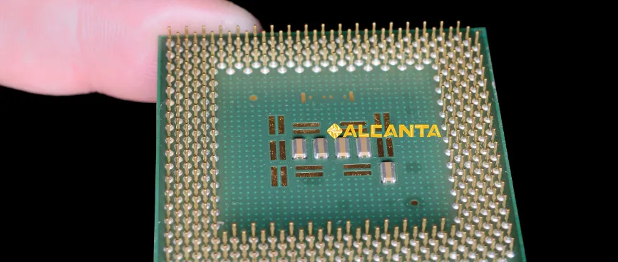
– High-Density Routing: HDI substrates incorporate microvias, fine lines, and high-density interconnections, allowing for more compact layouts and efficient use of space on the PCB.
– Compact Size: Due to their advanced manufacturing techniques, HDI substrates enable significant miniaturization without compromising performance, making them ideal for applications where space is limited.
– Lightweight Construction: The use of thin materials and advanced layering technologies results in lightweight HDI substrates, contributing to overall weight reduction in electronic devices.
Understanding these characteristics is essential for appreciating how HDI substrates contribute to the development of smaller, faster, and more reliable electronic products.
Composition of HDI Substrate Materials
Types of Materials Used
HDI substrates utilize a variety of materials tailored to meet specific performance requirements:
– High-Frequency Ceramics: These materials are valued for their excellent electrical properties, such as low dielectric loss and high thermal conductivity. They are ideal for applications requiring high-frequency signals and signal integrity, such as in telecommunications and radar systems.
– Polyimides (PI): Known for their high mechanical strength, thermal stability, and flexibility, polyimides are commonly used in HDI substrates where resilience to heat and mechanical stress is crucial. They are suitable for applications in aerospace, automotive electronics, and medical devices.
– FR-4 and BT Resins: These traditional PCB materials are also adapted for use in HDI substrates, offering cost-effectiveness and ease of manufacturing. They are suitable for less demanding applications where high-density interconnections are not critical.
Advantages and Applications
Each type of material offers distinct advantages that cater to different aspects of HDI substrate design:
– High-Frequency Ceramics: Provide superior signal integrity and thermal management, making them ideal for high-performance electronic devices and systems operating at GHz frequencies.
– Polyimides: Offer exceptional mechanical properties and chemical resistance, making them suitable for harsh environment applications where reliability and durability are paramount.
– FR-4 and BT Resins: Cost-effective and widely available, these materials are suitable for consumer electronics and applications where moderate performance requirements meet budget constraints.
By selecting the appropriate materials based on their unique properties, manufacturers can optimize the performance, reliability, and cost-effectiveness of HDI substrates for diverse electronic applications.
Manufacturing Process of HDI Substrates
Steps Involved in Multi-layer PCB Fabrication
The manufacturing process of HDI substrates involves several intricate steps to achieve high-density interconnections and compact design:
1. Layer Stackup Design: Engineers define the layer stackup considering the number of layers needed, material types for each layer, and the arrangement of conductive and insulating layers.
2. Inner Layer Processing: Thin copper foils are bonded to substrate materials such as polyimides or FR-4 using heat and pressure. Circuit patterns are then etched into the copper to create the inner layers of the PCB.
3. Via Formation: Microvias are drilled or laser-ablated to establish electrical connections between different layers. Sequential build-up (SBU) technology is often employed, where additional layers and vias are built up sequentially to achieve high-density routing.
4. Lamination: Layers of pre-impregnated resin and copper foil are pressed together under heat and pressure to form a solid multilayer structure. This process ensures reliable electrical connections and mechanical strength.
5. Surface Finishing: The final step involves applying surface finishes such as solder mask and metal finishes (e.g., gold, tin) to protect the PCB from oxidation, facilitate soldering, and ensure long-term reliability.
Impact on Performance and Reliability
The manufacturing processes significantly impact the performance and reliability of HDI substrates:
– Signal Integrity: Precise control over layer thickness, via size, and placement minimizes signal loss and interference, crucial for maintaining high-speed data transmission.
– Mechanical Durability: Advanced materials and lamination techniques enhance the PCB’s mechanical strength and resistance to thermal cycling, ensuring longevity in harsh operating conditions.
– Miniaturization: By enabling dense routing and compact designs, HDI substrate manufacturing processes support the trend towards smaller and more efficient electronic devices.
Understanding these manufacturing intricacies underscores the importance of choosing the right processes and materials to meet specific application requirements, ensuring optimal performance and reliability of HDI substrates in modern electronics.
Differences Between HDI Substrates and Traditional Non-HDI PCBs
Design and Performance Differences
HDI substrates differ significantly from traditional PCBs in several key aspects:
– Circuit Density: HDI substrates can achieve much higher circuit densities due to their use of microvias and fine line technology, allowing for more components and connections in a smaller footprint compared to traditional PCBs.
– Signal Integrity: The reduced size of microvias and advanced materials used in HDI substrates contribute to improved signal integrity by minimizing signal loss and noise, crucial for high-speed data transmission.
– Space Utilization Efficiency: HDI substrates maximize the use of available PCB space through compact designs and efficient routing, enabling manufacturers to create smaller and lighter electronic products without sacrificing functionality.
Advantages of HDI Substrates Over Traditional PCBs
HDI substrates offer several advantages that make them preferred for modern electronic applications:
– Enhanced Performance: Improved signal integrity and thermal management capabilities support higher performance requirements in advanced electronic devices.
– Miniaturization: Enables the development of smaller and more portable electronic products without compromising functionality or reliability.
– Reliability: The use of advanced materials and manufacturing techniques enhances the durability and longevity of HDI substrates, suitable for demanding applications in aerospace, telecommunications, and medical industries.
Understanding these differences and advantages helps stakeholders in the electronics industry make informed decisions when selecting PCB technologies that best suit their application needs and performance requirements.
Applications of HDI Substrates in the Electronics Industry
Specific Application Cases
HDI substrates find extensive use across various sectors within the electronics industry:
– Smartphones: HDI substrates enable the compact design and high-performance requirements of smartphones, supporting features like high-speed data transfer, miniaturized components (e.g., processors, memory), and multi-layered functionalities within a limited space.
– Laptops: In laptops, HDI substrates contribute to slim form factors and enhanced computing power by facilitating the integration of complex circuitry and high-speed interfaces while optimizing space utilization and thermal management.
– Communication Devices: HDI substrates play a crucial role in communication devices such as routers, modems, and network switches, ensuring reliable signal transmission, reduced latency, and efficient power consumption through advanced routing and signal integrity solutions.
Technological Innovations and Performance Enhancements
The adoption of HDI substrates in these applications leads to significant technological innovations and performance enhancements:
– Miniaturization: Allows for the development of thinner and lighter devices without compromising functionality, meeting consumer demand for portable and powerful electronics.
– High-Speed Data Transfer: Enables faster data transmission rates and lower latency, crucial for applications requiring real-time data processing and connectivity.
– Improved Reliability: Enhances the overall reliability and durability of electronic devices by minimizing signal interference, optimizing thermal management, and reducing the risk of mechanical failure.
By leveraging the capabilities of HDI substrates, manufacturers can achieve greater design flexibility, improved product performance, and enhanced user experiences across a wide range of electronic applications.
This expanded section highlights the critical role of HDI substrates in advancing technological capabilities and meeting the evolving demands of the electronics industry, from consumer electronics to specialized communication systems and beyond.
FAQs about hdi substrate
HDI (High Density Interconnect) substrate refers to a specialized type of printed circuit board (PCB) with densely packed components and intricate wiring patterns, allowing for compact designs and high-performance electronic devices.
HDI materials refer to the specific types of substrates and conductive materials used in manufacturing HDI PCBs. These can include high-frequency ceramics, polyimides, and other advanced materials tailored for high-density interconnections and miniaturization.
High Density Interconnect (HDI) substrates are PCBs designed with advanced interconnection technologies such as microvias, fine lines, and multiple layers to achieve high circuit density in a small area. They are crucial for modern electronics requiring compact size and enhanced performance.
The main differences lie in design complexity, circuit density, and manufacturing techniques:
– HDI PCBs use microvias and finer lines, allowing for more connections in a smaller space compared to non-HDI PCBs.
– Non-HDI PCBs typically have larger vias and are less dense, suitable for simpler electronic applications where compactness and high performance are not critical.
– HDI PCBs require advanced manufacturing processes and materials, contributing to higher cost but offering superior performance and miniaturization capabilities compared to non-HDI PCBs.

