
Key Design Tips for Effective Flexible PCB Prototyping
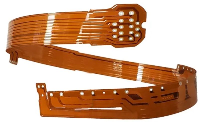
A Flexible PCB (Flex PCB) is a type of printed circuit board designed to bend, twist, or fold into shape without damaging the circuitry. Unlike rigid PCBs, flexible PCBs are built using materials like polyimide or polyester, making them ideal for applications requiring compact and dynamic configurations. Today, Flex PCBs are becoming increasingly essential in modern electronics such as wearable devices, medical equipment, aerospace systems, and compact consumer gadgets. Their ability to save space, reduce weight, and withstand mechanical stress makes them a preferred choice for innovative product designs. In this fast-paced tech landscape, flexible pcb prototyping plays a vital role in accelerating development cycles. Rapid prototyping allows engineers to validate designs quickly, identify potential issues early, and refine products before mass production. As demand for smarter, smaller, and more durable electronics rises, flexible pcb prototyping becomes a critical step in turning ideas into market-ready solutions.
Understanding Flexible PCBs for Flexible PCB Prototyping
Flexible PCBs are central to any flexible pcb prototyping workflow, and a clear grasp of their construction, applications, and trade-offs is essential for successful design.
Definition & Structure
A Flexible PCB is built on a thin, bendable substrate rather than the rigid FR-4 used in standard boards. Its basic layers include:
-
Polyimide base: The core flexible material, prized for thermal stability and chemical resistance.
-
Adhesive layer: Bonds the copper foil to the polyimide; typically acrylic or epoxy.
-
Copper foil: Forms the conductive traces; can be rolled annealed (RA) for better flexibility or electrodeposited (ED) for finer features.
-
Coverlay: A protective insulating film (often polyimide) laminated over copper to prevent damage and ensure reliability.
Rigid PCBs use thick fiberglass cores, while Flex PCBs eliminate rigid layers entirely. Rigid-Flex PCBs combine both: rigid sections for component mounting linked by flexible circuits for dynamic movement or three-dimensional assembly.
Typical Applications
-
Medical devices: Catheters, implantable sensors, diagnostic equipment
-
Automotive: Dashboard displays, lighting assemblies, sensor arrays
-
Consumer electronics: Wearables (smartwatches, fitness bands), foldable phones, compact cameras
-
Aerospace: Satellite systems, unmanned aerial vehicles, avionics modules
These sectors leverage the ability of flex circuits to conform to tight spaces and dynamic geometries where rigid boards cannot.
Advantages & Challenges
Advantages
-
Flexibility: Bends, folds, and twists enable creative packaging and three-dimensional layouts.
-
Lightweight: Thinner profiles reduce device weight and bulk.
-
Compact design: Eliminates the need for connectors and cables between rigid boards.
Challenges
-
Complex design rules: Requires careful consideration of bend radius, trace placement, and stress relief features.
-
Higher cost: Specialized materials and processes drive up per-unit pricing for prototypes.
-
Delicate manufacturing: Handling, drilling, and assembly demand tighter process controls to avoid tears, delamination, or pad lift-off.
Understanding these fundamentals ensures that engineers can optimize their designs and choose appropriate materials and processes for reliable flexible pcb prototyping.
Flexible PCB Prototyping Process for Flexible PCB Prototyping
A well-defined process is crucial when undertaking flexible pcb prototyping, ensuring your prototype meets both mechanical and electrical requirements before full production.
Design Phase
-
Design Tools:
-
Altium Designer: Industry-standard with built-in flex stackup wizards.
-
KiCad: Open-source option supporting bend line definitions.
-
Eagle: Lightweight tool with flex-friendly add-ons.
-
-
Design Considerations:
-
Bend Radius: Maintain a minimum bend radius at least ten times the total flex thickness to avoid trace cracking.
-
Trace Width & Spacing: Wider traces reduce stress; maintain standard clearances or tighter if your manufacturer allows it.
-
Stress Relief: Incorporate teardrops or mitered corners at pad-to-trace transitions and add relief slots in high-flex areas.
-
Impedance Control: For RF or high-speed signals, define controlled impedance layers in your stackup.
-
-
Reference: For detailed guidelines on defining bend zones and stress relief features, see Hemeixin PCB Design Tips.
Pre-Fabrication Preparation
-
Selecting a Manufacturer:
-
Evaluate capabilities: max layer count, material types (PI vs. PET), and minimum drill sizes.
-
Compare lead times, prototyping costs, and any prototyping-specific support services.
-
-
Required Design Files:
-
Gerber Files: Clearly mark coverlay openings and keep-out areas.
-
BOM: List all components, especially if using flexible-rated connectors or stiffeners.
-
Stack-Up Diagram: Specify material thicknesses and copper weights for each layer.
-
-
Technical Specifications:
-
Minimum Trace Width/Spacing: Often 4 mil/4 mil for flex; some vendors offer down to 3 mil/3 mil.
-
Minimum Drill Size: Typically 0.2 mm (8 mil) for standard flex, though microvias may be possible.
-
Layer Count: Keep prototypes simple (1–4 layers) to reduce complexity and cost; more layers can be prototyped but may increase risk of delamination.
-
By rigorously following these steps, engineers can minimize surprises during fabrication and ensure their flexible pcb prototyping yields a functional, reliable prototype.
Choosing the Right Prototyping Manufacturer for Flexible PCB Prototyping
Selecting the ideal partner is a critical step in flexible pcb prototyping, as each manufacturer offers distinct strengths, capabilities, and price points.
Manufacturer Overview & Comparison
-
PCBWay – Renowned for fast flexible PCB and Rigid-Flex turnaround, PCBWay supports up to 10 layers of polyimide flex, competitive volume pricing, and an intuitive online quoting system.
-
NextPCB – Provides end-to-end PCB plus SMT assembly services. Their prototyping package includes component sourcing and post-assembly testing, ideal for proof-of-concept builds.
-
JLCPCB – Offers some of the lowest prototype rates in the industry. With simple online ordering and 24-hour quote responses, JLCPCB is a go-to for startups and hobbyists on tight budgets.
-
Epec Tech – Specializes in high-reliability flex circuits for demanding environments. Their expertise in complex multilayer flex and controlled-impedance designs suits medical and aerospace applications.
-
Technotronix / Hemeixin / FlexPCB – Each provides customizable, high-performance flex services, including exotic materials (e.g., Rogers, Pyralux) and specialized processes like laser cutting and selective stiffener placement.
Quick Links to Supplier Pages:
Lead Time and Pricing
-
Typical Lead Times: Most prototyping services deliver within 3–7 working days. Expedited options (1–2 days) are available at a premium.
-
Cost Factors:
-
Material Selection: Polyimide and coverlay thickness, copper weight
-
Layer Count & Complexity: More layers and rigid-flex transitions increase tooling and inspection steps
-
Quantity & Delivery Speed: Small batch runs cost more per unit; rush orders incur express fees
-
By comparing these factors across providers, you can balance performance requirements against budget and schedule constraints to achieve successful flexible pcb prototyping outcomes.
A Brief Note on Rigid-Flex PCBs for Flexible PCB Prototyping
A Rigid-Flex PCB is a hybrid circuit combining traditional rigid board sections with integrated flexible interconnects. Layers of polyimide or polyester flex are laminated to FR-4 rigid cores, creating a single assembly that bends where needed while offering solid mounting areas.
When to Consider Rigid-Flex Over Fully Flexible PCBs
-
Mixed environment requirements: When components demand a stable mounting platform (e.g., heavy connectors or large BGAs) alongside dynamic flex zones.
-
Complex 3D assemblies: In compact products where fully rigid or fully flexible alone cannot meet spatial constraints.
-
Vibration and shock resistance: Rigid sections absorb mechanical stress, while flex sections reduce strain on solder joints.
Added Design & Manufacturing Complexity
-
Stackup intricacy: Multiple materials, varied dielectric thicknesses, and controlled impedance transitions between rigid and flex layers.
-
Advanced tooling: Precise registration, flex-to-rigid lamination, and specialized drilling for vias-in-pad and microvias.
-
Quality control: More inspection steps (e.g., dynamic flex testing, cross-section analysis) to verify integrity.
In many flexible pcb prototyping scenarios, Rigid-Flex boards offer the best of both worlds—but they require careful planning and collaboration with experienced manufacturers to ensure reliability and performance.
Common Issues & Best Practices in Flex PCB Prototyping for Flexible PCB Prototyping
Identifying common pitfalls and following proven design practices are essential for success in flexible pcb prototyping, where mechanical and electrical reliability must coexist in compact, often dynamic environments.
Frequent Issues
During flexible pcb prototyping, designers and fabricators frequently encounter the following issues:
-
Open/Short Circuits: Caused by hairline fractures in the copper traces or bridging due to inadequate spacing, especially in high-density layouts.
-
Warping: Irregular shrinkage or tension in laminated layers can lead to board deformation, making assembly and fitting into enclosures difficult.
-
Delamination: Poor adhesion between copper and substrate or improper curing of adhesives can cause layer separation under thermal or mechanical stress.
-
Pad Lift-Off: Bending or rework stress can detach pads from the flex substrate, especially where surface-mount components are involved.
Optimization Tips
To minimize these issues, implement the following best practices throughout your flexible pcb prototyping process:
-
Use Strain Relief in Bend Areas: Add fillets, anchor pads, or curved transitions at trace terminations to reduce mechanical stress concentration. Avoid placing vias or components in high-bend regions.
-
Avoid Sharp Corners in Traces: Use smooth, curved routing instead of 90-degree or acute angles. Sharp turns act as stress risers and increase the likelihood of trace cracking over time.
-
Choose Suitable Materials:
-
Polyimide: Offers superior thermal, chemical, and mechanical resistance. Ideal for dynamic applications and multilayer flex designs.
-
PET (Polyester): Cost-effective and adequate for static or limited-flex applications, but not recommended for repeated bending or high-heat environments.
-
By proactively addressing these issues and integrating thoughtful design decisions, engineers can significantly increase the success rate and durability of their flexible pcb prototyping projects.

