• FC-BGA substrate

How FC-BGA Substrate Enhances Performance in Modern Devices

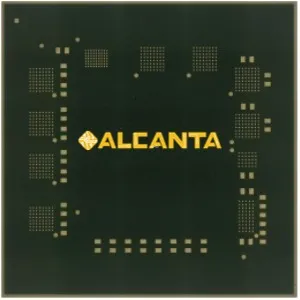
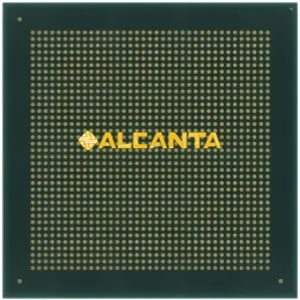
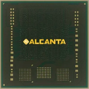
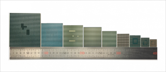
FC-BGA substrate uses advanced multilayer stacking technology with over 16 layers to achieve ultra-fine circuits under 10μm. It supports solder bumps smaller than 130μm and allows for large substrate sizes exceeding 60x60mm. This design enables high-density interconnections, improving electrical performance and thermal management. These features make FC-BGA substrate a preferred choice for packaging high-performance chips like CPUs, GPUs, and AI processors in modern electronics.

fc bga substrate-1

Online Consultation or Need a Quote

What is FC-BGA Substrate?

Definition of FC-BGA (Flip-Chip Ball Grid Array)

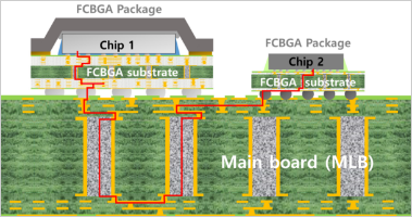
FC-BGA (Flip-Chip Ball Grid Array) is an advanced semiconductor packaging technology where the chip is “flipped” upside down and attached to a substrate via small solder bumps, or balls, arranged in a grid pattern. The solder bumps replace traditional wire bonds, allowing the chip to make direct electrical contact with the substrate. This method enhances the performance and reliability of the package while reducing its footprint. FC-BGA is commonly used in high-performance applications such as smartphones, computers, and automotive electronics, where space is limited, and efficiency is crucial.

FC-BGA’s Role in Modern Electronics

In today’s electronic devices, performance and miniaturization are at the forefront. FC-BGA substrates play a critical role by offering faster signal transmission, better heat management, and a more compact design. Since FC-BGA directly connects the chip to the PCB through solder bumps, it improves electrical performance and reduces the length of interconnections, which is important for high-speed applications. The packaging also helps manage heat more efficiently, making it ideal for devices that require continuous, high-performance operation, such as processors, memory modules, and high-definition graphics chips.

How FC-BGA Differs from Other Packaging Technologies

FC-BGA stands out in comparison to other packaging technologies like traditional BGA (Ball Grid Array) and CSP (Chip-on-Substrate).

  • BGA: In a traditional BGA, the chip is typically attached to the PCB using wire bonding, which can take up more space and have longer interconnections. While BGA still offers reliable connections, it is less efficient for high-speed, high-performance devices compared to FC-BGA, which uses solder bumps to directly connect the chip to the substrate for improved electrical and thermal performance.
  • CSP: Chip-on-Substrate (CSP) is another packaging method where the chip is directly mounted onto a substrate. However, CSP packages are often larger in size and may not provide the same level of performance, thermal management, or miniaturization as FC-BGA. FC-BGA, by contrast, offers a smaller, more efficient solution, especially for applications requiring high-density interconnections and superior heat dissipation.

In essence, FC-BGA combines the best features of these technologies, offering higher performance, better thermal management, and a compact form factor, making it the go-to choice for today’s advanced electronics.

The Role of FC-BGA Substrate

Explanation of the Substrate in FC-BGA Packages

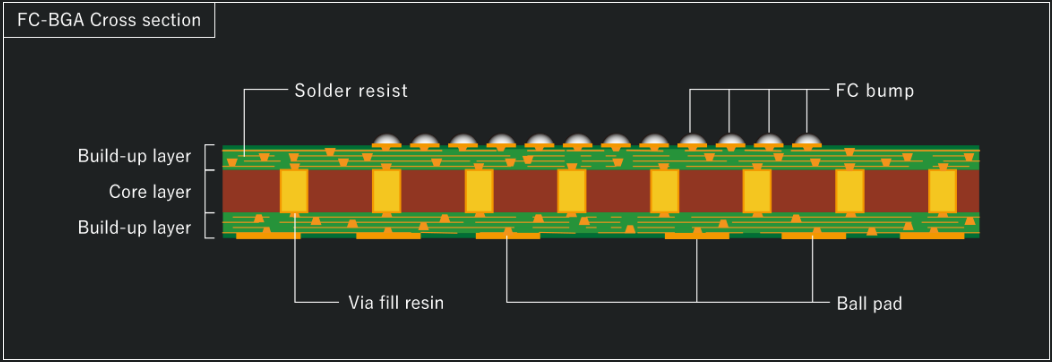
The substrate in FC-BGA packages is a critical component that supports the chip and provides the necessary infrastructure for electrical connectivity. Made from materials like organic laminates, ceramics, or metals, the FC-BGA substrate acts as a platform that connects the integrated circuit (IC) to the printed circuit board (PCB) of the electronic device. This substrate has several layers, including the base material, copper traces, and often an interposer layer to facilitate electrical connections between the chip and the PCB. The design of the substrate ensures that the chip is securely mounted while also providing pathways for electrical signals and power distribution.

How the Substrate Provides Mechanical Support and Electrical Connectivity

In FC-BGA packages, the substrate plays a dual role by offering mechanical support and ensuring electrical connectivity. Mechanically, it keeps the chip firmly in place, helping to prevent damage from external forces or vibrations. The solder bumps used in FC-BGA create a direct connection between the chip and the substrate, which in turn connects to the PCB. This direct connection not only strengthens the bond between the chip and the PCB but also allows for much higher-density interconnections compared to older packaging methods, such as wire bonding. The substrate’s role in electrical connectivity is vital as it routes signals, power, and ground connections from the chip to the external circuitry, ensuring seamless communication within the device.

Importance of the Substrate in Heat Dissipation and Electrical Performance

The substrate is essential in managing heat and improving the overall electrical performance of the FC-BGA package. During operation, electronic components generate heat, and the FC-BGA substrate is designed to help dissipate that heat efficiently to prevent overheating, which could lead to performance degradation or failure. The material selection for the substrate plays a big role here, with high-thermal conductivity materials like copper or ceramics helping to spread heat away from the chip. In addition, the substrate’s design is crucial for ensuring low electrical resistance and maintaining signal integrity, which is especially important for high-speed, high-frequency applications. Proper thermal management and excellent electrical performance are key factors in the reliability and efficiency of the final electronic device, making the substrate in FC-BGA packages indispensable for modern electronics.

Materials Used in FC-BGA Substrate

Common Materials for FC-BGA Substrates

The FC-BGA substrate is made from a variety of materials, each selected based on the specific needs of the application, such as performance, reliability, and cost. The most common materials used in FC-BGA substrates include organic laminates, ceramics, and metal cores.

  1. Organic Laminates: These are the most widely used material in FC-BGA substrates, consisting of layers of resin and glass fiber. Organic laminates provide an excellent balance between performance, cost, and manufacturability. They are typically used for mainstream electronics where high density and good thermal management are required, but extreme performance is not the primary concern.
  2. Ceramics: Ceramic substrates are often used in high-performance applications, such as in aerospace, automotive, and high-frequency RF (Radio Frequency) devices. Ceramics offer excellent thermal conductivity and high dielectric strength, making them ideal for handling higher power and heat dissipation. However, ceramics are more expensive and fragile compared to organic laminates, which limits their use to niche, high-end applications.
  3. Metal Cores: Metal-core substrates, which incorporate a metal base (often copper) with insulating layers, are used when additional heat dissipation is required. These substrates are particularly effective in power electronics and LED lighting, where efficient heat management is critical. While offering superior heat dissipation, metal-core substrates are generally more expensive and may have limitations in terms of electrical performance compared to organic laminates.

Why Laminate is the Most Commonly Used Material in FC-BGA

Organic laminate is the most commonly used material for FC-BGA substrates due to several advantages that make it well-suited for the majority of semiconductor packaging applications. First and foremost, organic laminates are cost-effective compared to ceramics or metal-core materials, making them ideal for mass production. They also offer good electrical performance and thermal conductivity, which are sufficient for most consumer electronics and general-purpose applications.

Another key reason for the widespread use of organic laminates in FC-BGA substrates is their flexibility in design and manufacturing. The resin and glass fiber composite materials can be easily shaped and fabricated into complex multi-layer structures, allowing for high-density interconnections and intricate routing of signals. This flexibility makes them perfect for the diverse and ever-evolving needs of modern electronics.

Properties That Make Laminate a Preferred Material for High-Performance Applications

The properties of organic laminates make them especially suitable for high-performance FC-BGA packages. Some of these properties include:

  • Thermal Management: While not as thermally conductive as ceramics or metal-core materials, organic laminates still provide adequate heat dissipation for most consumer and industrial applications. They can be engineered with additional heat sinks or thermal vias to improve thermal conductivity.
  • Electrical Performance: Organic laminates offer low electrical resistance and high signal integrity, which is crucial for maintaining fast and reliable communication between the chip and the PCB. They can be optimized for high-frequency performance, which is increasingly important as devices become more complex and data transfer speeds increase.
  • Mechanical Strength: Organic laminates provide the mechanical support necessary to secure the chip in place, preventing damage from external forces or vibrations. The material’s robustness is ideal for consumer electronics, where durability and reliability are essential.
  • Cost-Effectiveness: Compared to ceramics and metal-core substrates, organic laminates are much more affordable, making them the preferred choice for high-volume production, especially in consumer electronics like smartphones, computers, and wearables.

The combination of cost-effectiveness, reliable thermal and electrical performance, and design flexibility make organic laminates the go-to material for FC-BGA substrates in high-performance applications. This material allows manufacturers to meet the demanding requirements of modern electronic devices while balancing production costs and performance.

Structure and Design of FC-BGA Substrate

Description of the Different Layers in an FC-BGA Substrate

The structure of an FC-BGA substrate is complex and multi-layered, designed to support the flip-chip technology and provide the necessary electrical connections, thermal management, and mechanical stability. The key components of an FC-BGA substrate include the base layer, interposer, and copper traces.

  1. Base Layer: The base layer of an FC-BGA substrate is typically made from organic laminates, ceramics, or other materials that provide mechanical support. This layer serves as the foundation for all other layers, offering the structural integrity required to hold the chip in place and connect it to the printed circuit board (PCB). The base layer also helps with heat dissipation by providing a pathway for thermal management.
  2. Interposer: The interposer is an important layer that sits between the chip and the substrate, helping to route signals and power between the two. It ensures that the electrical connections are optimized, enabling high-density interconnections between the chip and the PCB. The interposer can be made from a variety of materials, including silicon or organic substrates, and often incorporates advanced features like microvias or through-silicon vias (TSVs) to support complex, high-speed connections.
  3. Copper Traces: Copper traces are the conductive pathways etched onto the substrate to carry electrical signals from the chip to the PCB. These traces are critical for ensuring the proper flow of electricity between the components. The traces are carefully designed and routed to minimize resistance and interference, which is especially important in high-frequency or high-performance applications. Copper traces are typically found in the interposer and base layers of the FC-BGA substrate.

Explanation of the Design Process: From the Chip to the Ball Grid Array and Substrate

The design of an FC-BGA substrate is a highly precise process that involves several key stages. First, the chip is flipped upside down, and its solder bumps or balls are aligned with the corresponding pads on the substrate. These solder bumps are then attached to the substrate through a process called “flip-chip bonding,” where the chip’s bumps are soldered directly onto the substrate’s pads, creating the electrical connections.

Once the chip is securely attached, the substrate’s interposer layer helps route the electrical signals from the chip’s pads to the copper traces in the base layer. These copper traces are then connected to the ball grid array (BGA) on the bottom of the substrate. The BGA consists of an array of solder balls arranged in a grid pattern, which will ultimately be soldered to the PCB. This connection allows for the transfer of data and power between the IC and the rest of the electronic system.

The design process also includes detailed planning for thermal management and signal integrity, ensuring that the chip’s performance is optimized. Thermal vias and heat sinks are incorporated into the design to direct heat away from the chip, preventing overheating and ensuring reliable operation.

The Role of the Underfill Material in Ensuring Reliability

Underfill material is a critical component in ensuring the long-term reliability of FC-BGA substrates. This material is used to fill the space between the chip and the substrate after the flip-chip bonding process. It serves several important purposes:

  1. Mechanical Support: Underfill material helps to distribute the mechanical stress across the substrate, reducing the risk of solder joint failure due to thermal cycling or mechanical shock. This is particularly important for FC-BGA packages that are used in environments where temperature changes or physical impacts are common.
  2. Thermal Management: The underfill material also plays a role in heat dissipation by filling the gap between the chip and the substrate. It helps transfer heat away from the chip, preventing hot spots that could lead to overheating and performance degradation.
  3. Improved Electrical Performance: The underfill material can help improve the electrical performance of the FC-BGA by reducing the risk of short circuits between the chip’s solder bumps and the substrate. It also prevents moisture or other contaminants from entering the gaps and affecting the chip’s functionality.
  4. Enhancing Reliability: By providing mechanical stability, reducing thermal stress, and preventing damage from environmental factors, underfill materials significantly enhance the overall reliability of the FC-BGA substrate. This is especially important for devices that require long-term durability and consistent performance, such as those used in automotive, aerospace, and industrial applications.

The design of an FC-BGA substrate involves multiple layers that work together to provide mechanical support, electrical connectivity, and thermal management. The underfill material plays a vital role in ensuring the reliability and longevity of the substrate, making FC-BGA a robust choice for high-performance electronic applications.

Get a Quotation For FC-BGA substrate Now

FC-BGA Substrate vs BGA and FCCSP: Key Differences

Comparison Between FC-BGA, Traditional BGA (Ball Grid Array), and FCCSP (Flip Chip Chip Scale Package)

When comparing FC-BGA substrate to traditional BGA (Ball Grid Array) and FCCSP (Flip Chip Chip Scale Package), the primary differences lie in their design, performance, and application suitability. Each packaging technology has its unique characteristics that make it suitable for different types of electronic devices and performance requirements.

  1. Traditional BGA (Ball Grid Array):
    Traditional BGA is one of the most widely used packaging technologies. In a standard BGA, the chip is connected to the PCB through wire bonds, and the solder balls on the underside of the package allow for easy connections to the board. BGA packages are relatively easy to manufacture and cost-effective, making them suitable for a wide range of applications, especially in consumer electronics.

    • Key Features: Wire bonds, solder balls, good for medium to low-density interconnections.
    • Limitations: BGA packages require more space than FC-BGA, leading to less efficient use of area and lower performance in high-speed, high-density applications. The wire bond connections are longer, which can negatively impact signal integrity and thermal management.
  2. FC-BGA (Flip-Chip Ball Grid Array):
    The FC-BGA substrate, as discussed earlier, uses flip-chip technology, where the chip is mounted upside down and connected to the substrate via solder bumps. This eliminates the need for wire bonding, providing more compact packaging and more efficient electrical connections. FC-BGA is ideal for high-performance applications where speed, size, and thermal performance are critical.

    • Key Features: Flip-chip technology, direct chip-to-substrate connection via solder bumps, high-density interconnects.
    • Advantages: Provides better electrical performance, improved heat dissipation, and is more compact. FC-BGA can support high-density interconnections, making it suitable for advanced processors, memory chips, and high-performance applications.
    • Limitations: More complex and expensive to manufacture compared to traditional BGA. The use of flip-chip bonding and underfill materials adds to the cost and complexity.
  3. FCCSP (Flip Chip Chip Scale Package):
    The FCCSP is similar to FC-BGA in that it uses flip-chip bonding to attach the chip to the substrate. However, FCCSP typically refers to packages where the size of the package is very close to the size of the chip itself (hence the term “chip-scale”). The distinction between FC-BGA and FCCSP is that FCCSP often omits the BGA balls and directly attaches to the PCB using solder bumps or other methods.

    • Key Features: Flip-chip technology, no BGA balls, compact design.
    • Advantages: Smaller than FC-BGA, offering a “near-chip scale” solution. It is suitable for applications where space is at a premium, such as mobile devices or small, portable electronics.
    • Limitations: The lack of BGA balls can limit the package’s ability to handle high-density interconnections. Additionally, thermal management can be a challenge, as the small package size limits heat dissipation capacity.

Advantages and Disadvantages of FC-BGA Over Other Packaging Technologies

The FC-BGA substrate has distinct advantages over both traditional BGA and FCCSP, but it also comes with its own set of challenges.

Advantages of FC-BGA:

  1. Performance: FC-BGA offers superior electrical performance due to the direct connection between the chip and the substrate via solder bumps. This reduces the electrical path length, enhancing signal integrity and minimizing transmission delay, making it ideal for high-speed data applications.
  2. Size Efficiency: FC-BGA allows for a much more compact design compared to traditional BGA, which uses wire bonding. The elimination of wire bonds in FC-BGA leads to a smaller package, which is especially beneficial in devices with space constraints.
  3. Thermal Management: The direct contact between the chip and substrate in FC-BGA enables better heat dissipation compared to traditional BGA, where heat can be trapped within the wire bonds. The FC-BGA’s design can incorporate additional thermal vias and other features to effectively manage heat, crucial for high-power devices like processors and GPUs.
  4. Density: FC-BGA supports high-density interconnections, making it well-suited for advanced semiconductor devices that require many connections in a small footprint. This is essential for modern electronics that demand both high performance and miniaturization.

Disadvantages of FC-BGA:

  1. Cost and Complexity: The manufacturing process for FC-BGA is more complex and costly than traditional BGA. The flip-chip bonding and underfill materials add extra steps to the production process, making it a more expensive option, especially for mass-market consumer products.
  2. Reliability Concerns: While FC-BGA offers excellent electrical performance, the flip-chip bonding process can sometimes lead to mechanical stresses, especially in applications that experience thermal cycling. The use of underfill materials helps mitigate this, but it adds complexity and can affect long-term reliability if not implemented correctly.

Advantages of Traditional BGA:

  • Cost-Effective: Traditional BGA packages are cheaper to manufacture and easier to assemble, making them ideal for high-volume production, especially in consumer electronics like smartphones, TVs, and laptops.
  • Simpler Manufacturing: The process of bonding wires and placing the chip on the substrate is relatively straightforward compared to flip-chip packaging.

Disadvantages of Traditional BGA:

  • Lower Performance: Traditional BGA’s wire bonding leads to longer electrical paths, which can result in slower data transfer speeds and reduced signal integrity. It also tends to take up more space, which is a drawback in miniaturized devices.
  • Thermal Issues: The additional length of wire bonds in BGA packages can hinder heat dissipation, making thermal management more challenging in high-performance applications.

Advantages of FCCSP:

  • Compact Size: FCCSP is often the smallest of the three options, making it ideal for devices where every millimeter of space matters, such as wearables or ultra-compact mobile devices.
  • Direct Chip-to-Board Connection: Like FC-BGA, FCCSP uses flip-chip bonding, ensuring excellent electrical performance and reduced package size.

Disadvantages of FCCSP:

  • Limited Density: FCCSP typically does not have the BGA ball grid, meaning it may be less suitable for high-density interconnects compared to FC-BGA.
  • Thermal Management Challenges: While compact, FCCSP’s small size can limit its ability to effectively manage heat, which could lead to overheating in high-power applications.

Focus on Performance, Size, and Thermal Management Capabilities

  • Performance: FC-BGA substrates excel in performance due to the direct chip-to-substrate connection, which allows for faster data transfer speeds, minimal signal interference, and greater electrical efficiency. Traditional BGAs, with their wire bonding, tend to suffer from longer electrical paths, which can degrade performance, especially at high frequencies.
  • Size: FC-BGA offers a more compact design than traditional BGA, which is essential as electronic devices continue to shrink in size. FCCSP takes size efficiency a step further, but this can come at the expense of performance and thermal management capabilities.
  • Thermal Management: FC-BGA substrates provide better heat dissipation than BGA due to the direct chip-to-substrate connection and design flexibility that allows for additional thermal features like vias and heat sinks. FCCSP, being smaller, faces more challenges in thermal management, while traditional BGA often requires additional components for effective heat dissipation.

FC-BGA substrates offer significant advantages over traditional BGA and FCCSP in terms of performance, size, and thermal management, making them ideal for high-performance applications. However, the complexity and cost of manufacturing FC-BGA packages must be considered when deciding between these packaging options.

FC-BGA Substrate vs PCB: What’s the Difference?

Clarifying the Difference Between a PCB (Printed Circuit Board) and an FC-BGA Substrate

At first glance, both a PCB (Printed Circuit Board) and an FC-BGA substrate might seem like similar components in the world of electronics, but they serve very different roles in the packaging and assembly of semiconductor devices.

A PCB is a flat, rigid or flexible board that holds and connects electronic components, such as resistors, capacitors, and integrated circuits (ICs). PCBs are the backbone of most electronic systems, providing the electrical paths that connect components to each other, and they typically consist of a base material, such as fiberglass, with copper traces to facilitate the flow of electricity. PCBs can range from simple single-layer designs to complex multi-layer configurations, depending on the complexity of the device.

An FC-BGA substrate, on the other hand, is a more specialized part of the packaging process used in high-performance integrated circuits (ICs). The FC-BGA substrate serves as the interface between the semiconductor chip and the PCB. The FC-BGA substrate itself provides the mechanical support, electrical connections, and heat dissipation for the chip through solder bumps (or balls) that directly connect the chip to the substrate. In essence, the FC-BGA substrate is not the primary board that houses and connects all the electronic components but a specific, often more complex package used to connect the chip to the PCB, ensuring proper performance and reliability.

The Role of PCB in the Larger System and How FC-BGA Fits Within That Structure

In any electronic system, the PCB acts as the main structural platform that interconnects various components such as processors, memory modules, and peripheral devices. The PCB’s job is to route electrical signals and power across these components, acting as the central nervous system of the device. It also often handles thermal management by providing pathways for heat dissipation and grounding for components.

An FC-BGA substrate is designed to sit between the chip and the PCB, ensuring that the chip can be effectively integrated into the broader system. The FC-BGA package allows the chip to connect to the PCB through the array of solder balls on the bottom of the substrate. When the FC-BGA is mounted onto the PCB, these solder balls are reflowed to make electrical connections, allowing data and power to flow between the chip and the rest of the circuit system.

The PCB provides the larger framework and physical layout for the entire device, while the FC-BGA substrate provides a more specific, specialized connection point for high-performance chips. The FC-BGA enables faster signal transmission, higher density interconnections, and more efficient heat dissipation, which are critical for modern, high-performance applications such as processors, memory, and graphics chips.

How the FC-BGA Substrate Differs in Design, Function, and Application from a Typical PCB

While the PCB serves as the foundation for electronic systems, the FC-BGA substrate is a specialized package that offers a range of enhancements in terms of performance, size, and thermal management.

  1. Design Differences:
    • A PCB typically has a much larger footprint and simpler design than an FC-BGA substrate. PCBs often have multiple layers to support the routing of signals, but these are usually made from standard materials like fiberglass or composite laminates. On the other hand, an FC-BGA substrate is designed with multiple complex layers, including copper traces, interposers, and sometimes even microvias to support high-density interconnections. This allows the FC-BGA to handle the advanced needs of high-speed, high-performance semiconductor devices.
    • The FC-BGA substrate also incorporates solder balls or bumps on the bottom, which are critical for the direct chip-to-substrate connection, something a typical PCB does not have.
  2. Function Differences:
    • The primary function of a PCB is to provide electrical paths and mechanical support for a variety of components. It’s essentially the main platform where various devices interact and communicate with each other within a system.
    • The FC-BGA substrate, in contrast, is specifically focused on connecting the chip to the PCB and handling high-speed signals, power distribution, and heat dissipation for that particular chip. It ensures that the chip can be reliably attached to the PCB and functions at optimal performance, especially in applications requiring high-speed data processing, such as CPUs, GPUs, and memory modules.
  3. Application Differences:
    • PCBs are used in virtually all types of electronic devices, ranging from simple gadgets to complex systems like computers, medical equipment, and automotive electronics. They can support a wide range of components and have designs that cater to many different use cases.
    • FC-BGA substrates, on the other hand, are used primarily in high-performance electronics. They are essential in devices that require high data transfer rates, minimal signal loss, and efficient heat management. Examples of applications include high-end processors, graphic cards, memory modules, and network communication devices. The FC-BGA package is often used in more advanced systems like smartphones, gaming consoles, servers, and automotive electronics that demand exceptional performance in compact form factors.

The PCB is the larger structural platform that interconnects all the components in an electronic device, while the FC-BGA substrate plays a much more specialized role, connecting high-performance chips to the PCB and ensuring their functionality in demanding applications. The FC-BGA substrate excels in areas like signal integrity, thermal management, and miniaturization, providing the required performance and reliability for modern, high-performance electronics.

Get a Quotation For FC-BGA substrate Now

Applications of FC-BGA Substrate: Key Use Cases and Future Trends

Use Cases in Consumer Electronics, Automotive, Telecommunications, and High-Performance Computing

The FC-BGA substrate is widely used in industries that require high-performance electronic devices with compact form factors, excellent heat dissipation, and minimal signal loss. Here’s how the FC-BGA substrate fits into several key sectors:

  1. Consumer Electronics:
    In consumer electronics, performance, size, and energy efficiency are crucial. Devices such as smartphones, tablets, gaming consoles, and wearables benefit greatly from FC-BGA packages due to their compact size and ability to handle high-speed processing with minimal heat buildup. The FC-BGA substrate is particularly useful in applications where space is limited, but performance cannot be compromised. For instance, in smartphones, the FC-BGA substrate is often used in high-performance processors and memory modules, allowing for powerful functionality in small devices.
  2. Automotive:
    The automotive industry increasingly relies on advanced electronics for applications like autonomous driving, infotainment systems, and electric vehicle (EV) powertrains. The FC-BGA substrate is essential in these systems because it provides both the electrical performance and thermal efficiency needed to manage the heat generated by power-hungry components like advanced driver-assistance systems (ADAS) processors, power management ICs, and electric motor controllers. With the growth of electric vehicles and connected car technologies, the demand for FC-BGA substrate in automotive applications is expected to rise.
  3. Telecommunications:
    The telecommunications sector, especially with the roll-out of 5G networks, relies on high-speed, high-density interconnections to support fast data transfer rates and connectivity. The FC-BGA substrate plays a key role in the development of telecommunications infrastructure, such as base stations, routers, and other networking equipment. High-performance chips used in 5G technology, including processors and RF (radio frequency) components, are often packaged using FC-BGA substrates to ensure that they can handle the high-speed data traffic and thermal demands of next-generation networks.
  4. High-Performance Computing (HPC):
    High-performance computing, including data centers, cloud computing, and artificial intelligence (AI) applications, demands the highest level of processing power. The FC-BGA substrate is widely used in these systems, especially in CPUs, GPUs, and memory chips. HPC applications require the combination of high density, speed, and effective heat dissipation, all of which are provided by FC-BGA packages. These substrates ensure that chips can perform at their highest capability without overheating, which is essential for tasks like machine learning, big data analytics, and scientific simulations.

Examples of Products That Commonly Use FC-BGA Packages

The FC-BGA substrate is commonly found in products that require compact, high-performance packages. Some specific examples include:

  1. Smartphones:
    The processors, memory, and other key components inside smartphones are often packaged using FC-BGA substrates. These substrates allow manufacturers to integrate powerful chips into slim, lightweight designs while ensuring the devices stay cool during heavy use, such as gaming or video streaming.
  2. Graphics Cards (GPUs):
    Graphics cards, especially those used in gaming, video editing, and scientific computing, utilize FC-BGA substrates for the GPUs. These processors require high-speed data transfer and efficient heat management, making FC-BGA an ideal solution for packing them into a compact, high-performance design.
  3. Servers and Data Centers:
    High-end servers and data centers that handle large-scale computing tasks such as cloud storage and AI workloads rely on FC-BGA substrates in their CPUs, memory modules, and networking chips. These systems require the highest level of processing power and thermal management, both of which are provided by FC-BGA packages.
  4. Autonomous Vehicles:
    In autonomous vehicles, FC-BGA substrates are used in the processors and sensors that handle real-time data processing for navigation, object detection, and decision-making. These systems must operate reliably in harsh conditions, making FC-BGA essential for high-performance and durability.
  5. 5G Equipment:
    As the demand for 5G infrastructure grows, telecommunications companies rely on FC-BGA substrates in the development of 5G base stations and other critical networking components. The ability of FC-BGA packages to manage heat and deliver high-speed signal transmission is key to supporting the high-frequency bands used in 5G.

Future Trends and Developments in FC-BGA Packaging

The FC-BGA substrate is expected to continue evolving, with several key trends emerging in its development:

  1. Smaller Form Factors:
    As devices continue to shrink in size, the demand for smaller and more compact FC-BGA packages will increase. Advanced packaging technologies, such as wafer-level packaging (WLP) and 3D stacking, are expected to be integrated with FC-BGA to achieve even smaller and more efficient designs.
  2. Higher-Density Interconnections:
    With the continued advancement of electronics, especially in areas like AI and 5G, the need for higher-density interconnects is crucial. The FC-BGA substrate is already capable of handling high-density connections, but future developments will push this even further to support even more complex devices. This may involve using advanced materials, such as high-performance laminates or embedded micro-vias, to improve the number of connections in a given space.
  3. Improved Thermal Management:
    As chips become more powerful, managing heat dissipation will become an even bigger challenge. FC-BGA substrates will continue to evolve with improved thermal management capabilities, including enhanced copper heatsinks, micro-channels, and advanced cooling techniques to ensure that high-power devices can operate without overheating.
  4. Integration with New Materials:
    The future of FC-BGA substrate packaging may involve integrating new materials that provide better performance, such as ceramics and advanced polymers, which could offer higher thermal conductivity, lower electrical resistance, and greater mechanical strength.
  5. Sustainability:
    With increasing attention on sustainability, FC-BGA packaging will likely see more focus on eco-friendly materials and manufacturing processes. This includes the development of materials that are recyclable or have a lower environmental impact during production.

The FC-BGA substrate is already integral to many high-performance electronic systems, and as technology continues to advance, its role will only expand. With the growing demands for faster, smaller, and more powerful electronics, the future of FC-BGA packaging promises even greater innovations, ensuring that it remains at the forefront of modern electronics packaging solutions.

Get a Quotation For FC-BGA substrate Now

Challenges and Limitations of FC-BGA Substrate: Overcoming Manufacturing and Cost Hurdles

Technical Challenges in Manufacturing FC-BGA Substrates

While FC-BGA substrates provide exceptional performance for high-end applications, their manufacturing process presents several technical challenges that need to be addressed to ensure the reliability and efficiency of the final product.

  1. Yield and Reliability Issues:
    The manufacturing process of FC-BGA substrates involves several complex steps, such as flip-chip bonding, solder bumping, and underfilling. These processes, while highly effective for high-performance chips, can result in low yield rates. A key issue is ensuring that all the solder bumps are perfectly aligned and connected to the chip and substrate. Misalignments, poor bonding, or incomplete connections can lead to electrical failures, impacting the overall reliability of the package. The high precision required for these steps makes the yield rate lower compared to more traditional packaging types, such as BGA.

    • Thermal Cycling and Stress: Another challenge in the reliability of FC-BGA substrates is the thermal cycling that occurs during use. When the device operates, it generates heat, which causes the chip and substrate to expand and contract. This thermal expansion can lead to mechanical stress on the solder bumps, potentially causing failures over time. The underfill material, used to protect the solder bumps, helps mitigate this issue, but it adds complexity and cost to the manufacturing process.
    • Microcracking: Over time, especially in high-stress environments like mobile devices or automotive applications, microcracks may form in the solder bumps due to thermal cycling or mechanical shock. These cracks can impair the electrical connection and eventually lead to failure of the chip. Ensuring long-term durability in such conditions remains a significant challenge for manufacturers of FC-BGA substrates.
  2. Process Complexity:
    The process of creating FC-BGA substrates involves sophisticated equipment for flip-chip bonding, high-precision solder ball placement, and careful underfilling of the chip to prevent thermal damage. This complexity makes the manufacturing process more susceptible to defects, and quality control is critical at every stage. Any variation in the process—whether in the alignment of bumps, underfill material distribution, or even slight imperfections in the substrate material—can lead to reduced performance or device failure.

Cost Considerations for Manufacturers and End Users

Manufacturing FC-BGA substrates comes with its own set of cost-related challenges that affect both producers and end users:

  1. Higher Manufacturing Costs:
    Due to the advanced materials and multi-step process involved, FC-BGA substrates are more expensive to produce than traditional BGA or CSP packages. The precision required for flip-chip bonding, solder bumping, and underfilling all contribute to higher manufacturing costs. Additionally, specialized equipment and expertise are needed, driving up the overall cost of production. These factors make FC-BGA packages more expensive than other traditional semiconductor packaging technologies, which can be a barrier for widespread adoption, especially in mass-market applications.
  2. Material Costs:
    The materials used in FC-BGA substrates—including high-performance laminates, ceramics, and specialized underfill compounds—are more costly than those used in traditional BGA substrates. The cost of these materials can significantly impact the final price of the packaged product. As FC-BGA substrates are commonly used in high-performance applications like CPUs, GPUs, and memory chips, the cost of materials must be considered in the context of the value these components bring to the end product.
  3. Cost for End Users:
    For the end user, products utilizing FC-BGA substrates typically come at a premium price due to the added manufacturing cost. However, this cost is often justified by the improved performance, reliability, and size efficiency that FC-BGA packaging offers, particularly in high-performance computing, telecommunications, and consumer electronics. Still, for industries that need to optimize costs without sacrificing too much performance, the higher price point of FC-BGA substrates might not always be justifiable, especially for devices that do not demand cutting-edge processing power.

Solutions to These Challenges Through Advancements in Material Science and Process Technology

As with many advanced technologies, FC-BGA substrates face challenges that are being actively addressed through innovations in material science and manufacturing processes.

  1. Advancements in Materials:
    A key solution to the reliability and thermal stress issues in FC-BGA substrates lies in the development of new materials that offer better mechanical properties and thermal conductivity. For instance, advanced underfill materials are being developed that provide greater flexibility and better protection for solder bumps, which can help prevent cracking and improve the overall lifespan of the package. Additionally, new ceramic or organic laminate materials with better thermal and electrical properties are being researched to enhance the performance of the substrate while reducing costs.
  2. Improved Bonding Technologies:
    As part of the effort to improve manufacturing yields, new bonding technologies such as micro-bump bonding and selective reflow processes are being explored. These techniques aim to improve the alignment and reliability of the solder bumps, minimizing the risk of defects during the bonding process. Innovations in flip-chip bonding technology also aim to make the process more precise and efficient, reducing both defects and production costs.
  3. Automated Manufacturing Processes:
    To address the cost and complexity of manufacturing FC-BGA substrates, manufacturers are turning to automated processes and AI-driven quality control systems. Automation can significantly reduce the labor costs and human error associated with traditional methods, improving yield rates and lowering the cost of production. Machine learning and AI are also being used to predict and correct issues in the manufacturing process before they lead to defects, which can further increase yield and reliability.
  4. Alternative Packaging Solutions:
    In response to the high costs and technical challenges associated with FC-BGA substrates, some manufacturers are exploring hybrid packaging solutions. These solutions combine the advantages of FC-BGA with more traditional packaging types, such as CSP (Chip-on-Substrate) or WLP (Wafer-Level Packaging), to balance performance, cost, and complexity. These hybrid solutions can reduce the overall expense of the packaging while still offering some of the key benefits of FC-BGA.
  5. Sustainability and Eco-Friendly Materials:
    As sustainability becomes a growing concern in the electronics industry, research into environmentally friendly materials for FC-BGA substrates is gaining momentum. Manufacturers are focusing on developing recyclable materials, reducing the use of hazardous substances, and optimizing production processes to minimize waste and energy consumption. These efforts can help reduce the environmental impact of FC-BGA substrates while still maintaining the high performance required for advanced applications.

While FC-BGA substrates present several challenges in terms of manufacturing complexity, yield, reliability, and cost, ongoing advancements in material science and process technology are helping to overcome these limitations. As these innovations continue to evolve, we can expect FC-BGA packaging to become more cost-effective, reliable, and accessible for a wide range of applications, driving further adoption in high-performance electronics.

FAQs About FC-BGA Substrate

FCBGA stands for Flip Chip Ball Grid Array, a type of electronic packaging where the silicon chip is flipped face-down onto the substrate, allowing for direct electrical connections. This method improves electrical performance and heat dissipation compared to other packaging types.

The main difference lies in the chip attachment method: in BGA (Ball Grid Array), the chip is mounted with the die facing up, and wire bonding is used to connect the die to the substrate. In contrast, FCBGA uses flip-chip technology, where the chip is mounted face-down, and solder bumps directly connect the die to the substrate. FCBGA offers better electrical performance and thermal management.

The substrate in a BGA package serves as the base that supports the chip and provides the electrical connections between the chip and the external circuitry. It is typically made from materials like FR-4 (a glass-reinforced epoxy laminate), which provides mechanical support and electrical insulation.

Flip chip substrates can be made from various materials, including FR-4, high-temperature FR-4, and polyimide (PI). The choice of material depends on the application’s thermal, electrical, and mechanical requirements.

FCBGA is preferred in high-performance applications because of its superior electrical performance, lower inductance and resistance, and enhanced thermal management. These characteristics make it suitable for high-speed and high-power devices.

FCBGA improves signal integrity by reducing the length of electrical paths between the chip and the substrate, which minimizes signal delay, distortion, and crosstalk. The direct solder bump connections also reduce parasitic inductance and capacitance.

The flip-chip design in FCBGA packages allows for efficient heat dissipation directly from the chip through the substrate. This design can include thermal vias and heat sinks, which help manage the heat generated by high-power components, enhancing reliability and performance.

FCBGA packages are commonly used in industries requiring high-performance electronic components, such as computing, telecommunications, aerospace, automotive, and industrial automation.

Challenges associated with FCBGA packaging include higher manufacturing costs, increased complexity in design and production, and the need for advanced materials and processes to handle the precise alignment and attachment of the chip to the substrate.

Trends in FCBGA technology development include the use of advanced materials for substrates, such as ceramics and organic substrates, the integration of thermal management solutions like liquid cooling, and the adoption of environmentally friendly manufacturing processes. Additionally, there is ongoing research into improving the reliability and reducing the costs of FCBGA packages.

Contact Us NOW