
FCCSP: Pioneering Compact Chip Solutions
Packaging technology plays a crucial role in the realm of integrated circuit design, serving as the bridge between the semiconductor chip and its environment. It encompasses the encapsulation and protection of the chip while facilitating electrical connections, thermal management, and overall functionality. Understanding the significance of packaging is essential, as it directly impacts the performance, reliability, and form factor of electronic devices.
Within this landscape, Flip Chip Chip Scale Package (FCCSP) technology emerges as a pivotal solution. Positioned at the forefront of packaging innovations, FCCSP offers a compact form factor, high-density interconnects, and efficient heat dissipation capabilities. Its versatility extends across diverse sectors, including mobile devices, telecommunications, automotive electronics, and more. By delving into FCCSP’s applications and market penetration, we can unravel its transformative potential in advancing integrated circuit design and shaping the future of electronics.
Overview of FCCSP Packaging
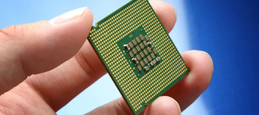
Flip Chip Chip Scale Package (FCCSP) represents a cutting-edge packaging technology revolutionizing the integrated circuit landscape. This sophisticated packaging method involves directly attaching the chip to the substrate, optimizing space utilization, and enhancing performance characteristics.
FCCSP’s design embodies several distinctive features and advantages. Firstly, its compact size allows for significant space savings, making it ideal for applications where real estate is limited. Additionally, FCCSP boasts high-density interconnects, facilitating enhanced electrical performance and signal integrity. This attribute is particularly advantageous in applications requiring intricate circuitry and high-speed data transmission.
Moreover, FCCSP excels in thermal management, efficiently dissipating heat generated by the semiconductor chip. This capability ensures optimal operating conditions, prolonging the lifespan and reliability of electronic devices. The combination of small form factor, high density, and superior thermal management positions FCCSP as a preferred packaging solution for a wide range of applications.
In the realm of mobile devices, FCCSP finds extensive use in smartphones, tablets, and wearables, where space constraints and performance demands converge. Its compact design enables manufacturers to create sleek and lightweight devices without compromising functionality. In communication equipment, FCCSP facilitates the development of high-performance routers, switches, and base stations, ensuring seamless connectivity and data transmission. Furthermore, FCCSP is prevalent in consumer electronics such as digital cameras, gaming consoles, and smart home devices, where its compact footprint and reliability are highly valued.
Overall, FCCSP emerges as a versatile and indispensable packaging technology, driving innovation across various industries and shaping the future of electronic devices. Its combination of small size, high density, and efficient thermal management makes it a preferred choice for designers seeking to optimize performance and functionality in space-constrained applications.
Comparison between FCCSP and WLCSP
Explain the full name of WLCSP: Wafer Level Chip Scale Package
Wafer Level Chip Scale Package (WLCSP) is a packaging technology where the chip is packaged at the wafer level before it is diced into individual units. This process allows for the integration of packaging and testing directly onto the wafer, reducing manufacturing costs and enabling smaller form factors.
Compare the characteristics and application areas of FCCSP and WLCSP
Both FCCSP and WLCSP are advanced packaging technologies renowned for their compact size and high-density interconnects. However, they differ in their manufacturing processes and application areas.
- Characteristics: FCCSP typically involves the attachment of the chip to a substrate, whereas WLCSP packages are formed directly on the wafer. FCCSP may offer slightly better thermal management due to the presence of a substrate, while WLCSP excels in miniaturization and potentially lower manufacturing costs due to its wafer-level process.
- Application Areas: FCCSP is commonly used in applications where space-saving is critical but where some level of substrate support is desirable, such as mobile devices, telecommunications equipment, and automotive electronics. On the other hand, WLCSP is favored in applications where the smallest possible form factor is essential, such as in wearable devices, IoT sensors, and medical implants.
Analyze the differences between the two in packaging technology, cost, reliability, etc.
- Packaging Technology: FCCSP involves attaching the chip to a substrate, which provides some structural support and thermal dissipation capabilities. In contrast, WLCSP directly packages the chip at the wafer level, eliminating the need for a separate substrate and potentially enabling smaller form factors. While FCCSP may offer slightly better thermal management, WLCSP excels in miniaturization and potentially lower manufacturing costs due to its wafer-level process.
- Cost: The cost of manufacturing FCCSP and WLCSP can vary depending on factors such as volume, complexity, and materials used. Generally, WLCSP may have a cost advantage due to its simplified manufacturing process and reduced material usage. However, FCCSP may offer better economies of scale for certain applications where substrate-based packaging is preferred.
- Reliability: Both FCCSP and WLCSP are known for their reliability, but they may exhibit differences in reliability performance depending on the specific application and environmental conditions. Factors such as thermal cycling, mechanical stress, and moisture sensitivity should be considered when evaluating the reliability of each packaging technology for a particular application.
Overall, the choice between FCCSP and WLCSP depends on factors such as space constraints, cost considerations, and specific performance requirements. Designers must carefully evaluate the trade-offs between these packaging technologies to select the most suitable option for their applications.
FCCSP Packaging Process
Introduce the manufacturing process of FCCSP packaging, including design, manufacturing, testing, and assembly
The manufacturing process of FCCSP packaging involves several key stages, each crucial for ensuring the reliability and performance of the final product.
- Design: The design phase begins with the selection of materials and the layout of the integrated circuit. Design considerations include electrical performance, thermal management, and mechanical robustness. Advanced CAD software is used to create the layout of the package, including the arrangement of interconnects and the placement of the semiconductor chip.
- Manufacturing: Once the design is finalized, the manufacturing process begins with the fabrication of the substrate. This may involve processes such as etching, deposition, and lithography to create the necessary features on the substrate. Next, the semiconductor chip is attached to the substrate using flip chip bonding techniques. This step requires precise alignment and bonding to ensure reliable electrical connections.
- Testing: After assembly, the FCCSP package undergoes rigorous testing to verify its functionality and reliability. This includes electrical testing to ensure proper connectivity and signal integrity, as well as thermal testing to evaluate the package’s ability to dissipate heat. Additional tests may be performed to assess the package’s resistance to mechanical stress, environmental factors, and other potential sources of failure.
- Assembly: Once testing is complete, the FCCSP packages are ready for final assembly into electronic devices. This may involve mounting the packages onto printed circuit boards (PCBs) and connecting them to other components using soldering or bonding techniques. Quality control measures are implemented throughout the assembly process to ensure consistency and reliability.
Discuss technical challenges and solutions that may be encountered in FCCSP packaging
While FCCSP packaging offers many advantages, several technical challenges may arise during the manufacturing process.
- Alignment and Bonding: Achieving precise alignment and bonding between the semiconductor chip and the substrate can be challenging, particularly for high-density interconnects. Advanced alignment techniques and bonding materials may be required to ensure reliable connections.
- Thermal Management: FCCSP packages must effectively dissipate heat generated by the semiconductor chip to prevent overheating and maintain optimal operating conditions. Innovative thermal management solutions, such as thermal vias and heat spreaders, may be employed to enhance heat dissipation capabilities.
- Reliability: Ensuring the long-term reliability of FCCSP packages requires careful attention to factors such as mechanical stress, thermal cycling, and environmental conditions. Robust design and manufacturing practices, as well as comprehensive testing protocols, are essential for identifying and addressing potential reliability issues.
- Miniaturization: As electronic devices continue to shrink in size, there is increasing pressure to miniaturize FCCSP packages even further. This requires innovative manufacturing techniques and materials to maintain reliability and performance in increasingly compact form factors.
Addressing these technical challenges requires collaboration between semiconductor manufacturers, packaging suppliers, and electronic device manufacturers. By leveraging advanced materials, processes, and design methodologies, FCCSP packaging can continue to evolve to meet the demands of next-generation electronic devices.
Application Cases of FCCSP Packaging
Provide several specific cases to demonstrate the application of FCCSP in real projects
- Smartphones and Tablets: FCCSP packaging is extensively used in smartphones and tablets to achieve compact form factors while maintaining high performance. For example, in flagship smartphones, FCCSP is employed to package the application processor, memory chips, and other key components. This enables manufacturers to create sleek and lightweight devices with advanced features.
- Wireless Communication Devices: FCCSP is widely adopted in wireless communication devices such as routers, modems, and access points. In these applications, FCCSP packages are used to house RF transceivers, baseband processors, and other critical components. The small size and high-density interconnects of FCCSP enable manufacturers to design compact and power-efficient communication devices for both consumer and industrial markets.
- Automotive Electronics: In the automotive industry, FCCSP packaging is utilized in various electronic systems, including advanced driver assistance systems (ADAS), infotainment systems, and engine control units (ECUs). FCCSP packages offer robustness and reliability, making them suitable for harsh automotive environments. They enable the integration of complex electronic systems into vehicles while meeting stringent size and performance requirements.
Analyze the advantages and value of FCCSP packaging in these cases
- Size and Weight Reduction: FCCSP packaging enables significant size and weight reductions in electronic devices, making them more portable and convenient for users. This is particularly valuable in applications such as smartphones and tablets, where compactness is essential for enhancing user experience.
- High-Density Interconnects: The high-density interconnects provided by FCCSP packaging allow for efficient routing of signals and power within electronic devices. This results in improved electrical performance and signal integrity, contributing to the overall reliability and functionality of the device.
- Thermal Management: FCCSP packages offer effective thermal management capabilities, ensuring that electronic components operate within their specified temperature ranges. This is critical for maintaining device performance and prolonging component lifespan, especially in applications where heat dissipation is a concern, such as automotive electronics.
- Reliability: FCCSP packaging is known for its reliability and robustness, making it suitable for demanding applications such as automotive electronics and communication devices. The flip chip bonding technology used in FCCSP packages provides strong mechanical connections, minimizing the risk of failure due to mechanical stress or thermal cycling.
In summary, FCCSP packaging offers numerous advantages across a wide range of applications, including size and weight reduction, high-density interconnects, efficient thermal management, and reliability. These benefits contribute to the overall performance, functionality, and user experience of electronic devices in various industries.
Future Development Trends
As technology continues to advance, the development of FCCSP packaging technology is expected to follow several key trends, shaping its future direction:
- Miniaturization and High-Density Integration: One of the primary trends in FCCSP packaging is the ongoing drive towards miniaturization and high-density integration. As electronic devices become smaller and more compact, there is a growing demand for packaging solutions that can accommodate increasingly complex circuitry in limited space. Future developments in FCCSP technology will focus on further reducing package size and increasing the density of interconnects to meet these demands.
- Advanced Materials and Manufacturing Processes: Another important trend in FCCSP packaging is the adoption of advanced materials and manufacturing processes to improve performance and reliability. This includes the use of new substrate materials with enhanced thermal and electrical properties, as well as the development of novel bonding techniques and assembly methods. Future innovations in materials and processes will enable the production of FCCSP packages with improved thermal management, higher reliability, and lower manufacturing costs.
- Enhanced Thermal Management Solutions: With the increasing power density of electronic devices, effective thermal management is becoming increasingly important in FCCSP packaging. Future developments in thermal management solutions will focus on improving heat dissipation capabilities and optimizing thermal pathways within the package. This may involve the integration of advanced thermal interface materials, heat spreaders, and thermal vias to enhance heat transfer and improve overall device reliability.
- Integration of Advanced Functionality: As the capabilities of electronic devices continue to expand, there is a growing need for packaging solutions that can support advanced functionality and features. Future developments in FCCSP technology will focus on integrating additional functionality into the package, such as embedded sensors, RF components, and power management circuitry. This will enable the development of highly integrated devices with enhanced performance and functionality.
- Emerging Applications and Markets: The growing adoption of FCCSP packaging technology is expected to open up new opportunities in emerging applications and markets. Future developments in FCCSP technology will enable its use in a wider range of applications, including wearable electronics, IoT devices, medical implants, and automotive electronics. This will drive continued growth and innovation in the FCCSP market, as manufacturers seek to capitalize on the benefits of this advanced packaging technology.
The future development of FCCSP packaging technology will be driven by trends towards miniaturization, advanced materials and manufacturing processes, enhanced thermal management solutions, integration of advanced functionality, and the emergence of new applications and markets. By staying at the forefront of these trends, manufacturers can continue to innovate and drive the evolution of FCCSP packaging technology to meet the needs of future electronic devices.


发表评论
Want to join the discussion?Feel free to contribute!