
Benefits of Embedded Cavity PCB Manufacturing
Embedded Cavity PCB Manufacturing is an advanced process that integrates components within recessed cavities in the PCB structure, enabling reduced board thickness, improved electrical performance, and better thermal management. As electronic devices continue to shrink while requiring higher functionality, embedded cavity PCBs have become a key solution in modern electronics.
We have produced Embedded Cavity PCB boards using cutting-edge technology, ensuring precise depth control and high-accuracy cavity sizes. Our capabilities range from 4-layer to 30-layer designs, meeting diverse application needs. By embedding components directly into the PCB, this technology enhances miniaturization, reliability, and performance, making it ideal for high-frequency, high-power, and mission-critical applications. Embedded Cavity PCB Manufacturing offers superior electromagnetic shielding, shorter interconnects, and improved mechanical stability.
What is an Embedded Cavity PCB?
Definition and Structural Characteristics
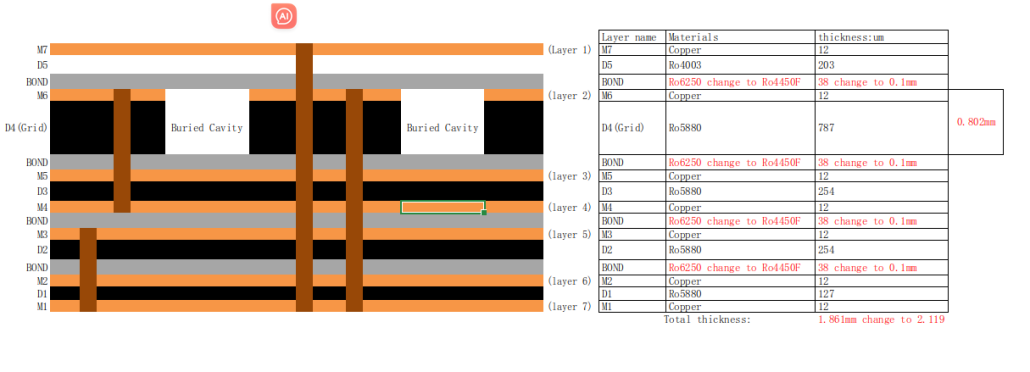
Embedded Cavity PCB is a specialized type of circuit board that features recessed cavities within its layers, allowing components to be placed inside rather than on the surface. This design reduces overall board thickness, enhances electrical performance, and improves heat dissipation. The cavities are precisely manufactured with controlled depth and dimensions to accommodate various embedded components, such as ICs, capacitors, and resistors.
Difference Between Traditional PCBs and Embedded Cavity PCBs
Unlike traditional PCBs, where all components are mounted on the surface, Embedded Cavity PCB Manufacturing integrates components within the board structure. This approach shortens signal paths, reduces electromagnetic interference (EMI), and improves mechanical stability. Additionally, embedded cavity PCBs offer better thermal management and a more compact design, making them ideal for high-density electronic systems.
Common Applications
Embedded cavity PCBs are widely used in advanced electronic applications, including RF modules, where reduced signal loss is critical. They are also essential in high-speed computing for improved electrical performance, medical devices requiring compact and reliable circuits, and aerospace applications demanding lightweight and durable solutions.

Get a Quotation For Embedded Cavity PCB Manufacturing Now
Manufacturing Process of Embedded Cavity PCB Manufacturing
PCB Material Selection
The choice of materials is crucial for Embedded Cavity PCB Manufacturing, as it directly impacts performance and reliability. Common materials include FR4, BT resin, and glass substrates, each offering different benefits for mechanical strength, thermal stability, and dielectric properties. Glass substrates, in particular, provide excellent dimensional stability, making them ideal for high-precision cavity structures. Proper material selection ensures precise cavity formation and long-term reliability.
Cavity Formation Methods
Creating cavities in PCBs requires advanced techniques to maintain precision and consistency:
-
Mechanical Milling: A cost-effective method ensuring controlled depth but with limitations in fine-pitch applications.
-
Laser Ablation: Provides high precision for intricate designs and minimizes mechanical stress.
-
Etching Techniques: Uses chemical processing for complex cavity geometries, suitable for high-density PCBs.
Embedding Components
Embedding components inside the cavity enhances performance and miniaturization. Key considerations include:
-
SMT vs. Bare-Die Embedding: Surface-mounted components are easier to integrate, while bare-die embedding allows for a lower profile.
-
Conductive Adhesives vs. Soldering Methods: Conductive adhesives reduce thermal stress, whereas soldering offers stronger electrical connections.
-
Thermal Management: Efficient heat dissipation is critical for high-power applications.
Multilayer Lamination Process
During lamination, layers with cavities must be precisely aligned to avoid defects. Key steps include:
-
Alignment Challenges: Ensuring accurate positioning of cavities and embedded components.
-
Pressing and Bonding: Optimizing pressure and temperature to maintain structural integrity.
-
Reliability Considerations: Preventing delamination and warping after lamination.
Electrical Interconnections
Reliable interconnections are essential for high-performance PCBs. Key techniques include:
-
Via Formation: Plated vias and buried vias ensure stable electrical pathways.
-
Copper Plating: Enhances conductivity and durability.
-
Testing Methods: Impedance testing and signal integrity analysis verify electrical performance.
Final Fabrication and Testing
The final stage of Embedded Cavity PCB Manufacturing includes finishing and quality checks:
-
Surface Finish Options: ENIG, ENEPIG, and OSP enhance solderability and longevity.
-
Functional Testing: Electrical testing ensures all embedded components operate correctly.
-
Quality Control: X-ray inspection and reliability tests confirm manufacturing accuracy.
Get a Quotation For Embedded Cavity PCB Manufacturing Now
Materials Selection for Embedded Cavity PCB
We offer a wide range of materials for Embedded Cavity PCB Manufacturing, ensuring high performance across various applications.
High-Frequency Materials
For RF and microwave applications, we manufacture cavity PCBs using advanced high-frequency materials, including:
RO Series: RO3003, RO3003G2, RO3006, RO3010, RO3035, RO3202, RO3203, RO3206, RO3210, RO3730, RO5780, RO5880, RO6002, RO6006, RO4003C, RO4232, RO4233, RO4360, RO4360G2, RO4400, RO4500, RO4533, RO4535, RO4700, RO4730, RO4830, RO4835T.
RT Series: RT5880, RT5870, RT6006, RT6010.
Other RF Materials: CLTE, Genclad, RF35, FastRise27, TLC, TLX, TLY, Taconic 601, 602, 603, 605.
High-Speed Core Materials
For high-speed digital applications, we utilize:
- Panasonic Megtron Series: Megtron4, Megtron6, Megtron7, Megtron7N.
- Other High-Speed Cores: TU872SLK, FR408HR, N4000-13 Series, MW4000, MW2000, TU933.
High-Performance & Low-Loss FR4 Materials
For demanding low-loss applications, we offer:
- High-Performance Cores: EMC EM828, EM827, EM888(S), EM888(K), Isola FR408, FR408HR.
- Low-Loss FR4: Isola I-Speed, I-Tera MT, Nelco N4000-13EP, EPSI, Panasonic R5775.
Advanced Manufacturing Capabilities
We specialize in high-precision cavity PCB fabrication, incorporating:
- Embedded vias: Buried, blind, and back-drilled vias.
- Hybrid Constructions: Mixed materials and dielectric combinations.
- Depth-Controlled Drilling & Routing: Ensuring exact cavity dimensions.
- Tight Impedance Control: ±10% or ±5% tolerance.
If your required PCB material is not listed, feel free to contact us for custom solutions.
Get a Quotation For Embedded Cavity PCB Manufacturing Now
Challenges in Embedded Cavity PCB Manufacturing
Design Complexity and DFM Considerations
Embedded Cavity PCB Manufacturing involves intricate design challenges that require careful Design for Manufacturability (DFM) considerations. Engineers must account for precise cavity depths, alignment of embedded components, and layer stack-up configurations to ensure functionality and reliability. Signal integrity is another key factor, as shorter interconnections improve performance but require meticulous routing to prevent signal interference. Additionally, compatibility with standard PCB fabrication processes must be evaluated to avoid excessive production costs and delays.
Thermal Expansion and Mechanical Stress
The integration of cavities and embedded components introduces challenges related to thermal expansion and mechanical stress. Different materials within the PCB—such as FR4, BT resin, and glass substrates—expand at varying rates under temperature fluctuations, potentially leading to warping, delamination, or microcracks. Effective thermal management solutions, such as advanced heat dissipation structures and optimized material selection, are essential to ensure the long-term reliability of the PCB, particularly in high-power and high-frequency applications.
Yield and Cost Challenges
Manufacturing yield is a critical factor in Embedded Cavity PCB Manufacturing, as defects in cavity formation, lamination, or embedding processes can lead to high scrap rates. Achieving tight tolerances for cavity depth and alignment increases production complexity, requiring advanced fabrication techniques and stringent quality control measures. Additionally, material costs, specialized equipment, and extended processing times contribute to higher overall manufacturing expenses. To optimize cost-effectiveness, manufacturers must balance precision, material efficiency, and process automation while maintaining high yield rates.
Contact Us NOW
FAQs About Embedded Cavity PCB Manufacturing
What is Embedded Cavity PCB Manufacturing?
Embedded Cavity PCB Manufacturing is a process that integrates recessed cavities within the PCB structure to embed components such as ICs, capacitors, or resistors. This technique reduces board thickness, improves electrical performance, and enhances thermal management.
What are the advantages of Embedded Cavity PCB Manufacturing?
The key benefits include miniaturization, better signal integrity due to shorter interconnects, improved electromagnetic shielding, enhanced thermal dissipation, and increased mechanical stability. These features make embedded cavity PCBs ideal for high-frequency and high-power applications.
How does material selection impact Embedded Cavity PCB Manufacturing?
Material selection plays a crucial role in Embedded Cavity PCB Manufacturing, affecting performance, durability, and manufacturability. High-frequency materials ensure minimal signal loss, high-speed cores support fast data transmission, and low-loss FR4 enhances electrical efficiency. The right materials also influence thermal expansion, cavity formation precision, and overall mechanical stability, making them critical for reliable embedded cavity PCB production.
What are the main methods used to create cavities in Embedded Cavity PCB Manufacturing?
The primary methods include mechanical milling for cost-effective depth control, laser ablation for high-precision cavities, and chemical etching for complex structures. Each method is chosen based on design complexity and production efficiency.
What are the main challenges in Embedded Cavity PCB Manufacturing?
Challenges include precise depth control, alignment of embedded components, thermal expansion mismatches, mechanical stress, and maintaining high manufacturing yield while keeping costs manageable. Advanced fabrication techniques and stringent quality control help overcome these challenges.

