
Small Yet Mighty: The Power of Chip Scale Packages
Chip Scale Package (CSP) technology plays a pivotal role in the miniaturization and enhancement of electronic devices across various industries. Its significance lies in its ability to offer compact packaging solutions without compromising performance, making it ideal for applications where space constraints are critical. In this article, we will delve into the fundamentals of CSP, exploring its evolution, manufacturing processes, and comparison with other packaging technologies. Additionally, we will examine the diverse application domains of CSP, ranging from mobile devices to automotive electronics, highlighting its versatility and impact. Through this exploration, readers will gain insights into the pivotal role of CSP in shaping the future of integrated circuit packaging.
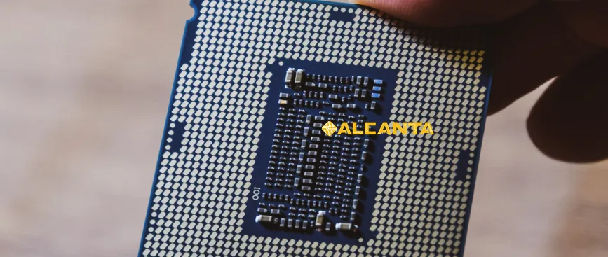
Introduction to Chip Scale Package (CSP)
Definition and Development History of CSP:
Chip Scale Package (CSP) is a cutting-edge packaging technology that revolutionizes the way integrated circuits (ICs) are encapsulated. Unlike traditional packaging methods that leave significant unused space, CSP encapsulates the IC chip with minimal extra material, resulting in a package size comparable to the chip itself. The concept of CSP emerged in the late 20th century as a response to the growing demand for smaller and more efficient electronic devices. Over the years, CSP has evolved significantly, with advancements in manufacturing processes and materials, leading to improved performance and reliability.
The Role and Significance of CSP in the Field of Integrated Circuit Packaging:
CSP plays a pivotal role in addressing the ever-increasing demand for miniaturization in electronic devices. Its significance lies in its ability to provide high-density packaging solutions while maintaining excellent electrical and thermal performance. By eliminating the need for additional packaging materials and reducing the distance between the chip and the circuit board, CSP enables faster signal transmission and more efficient heat dissipation. Moreover, CSP facilitates cost reduction in manufacturing due to its simplified assembly process and reduced material usage. As a result, CSP has become the go-to packaging technology for a wide range of applications, including smartphones, wearables, automotive electronics, and more.
Process of CSP
Overview of Wafer Level Packaging (WLP) Process:
Wafer Level Packaging (WLP) is a key process in the manufacturing of Chip Scale Packages (CSP). Unlike traditional packaging methods where individual IC chips are packaged after wafer fabrication, WLP involves encapsulating the chips directly on the wafer itself. This process eliminates the need for dicing and handling individual chips, leading to higher efficiency and lower costs. WLP typically utilizes thin-film deposition, photolithography, and etching techniques to create the necessary interconnects and protective layers directly on the wafer.
Key Steps in CSP Manufacturing Process:
1. Wafer Processing: The process begins with the fabrication of semiconductor wafers using standard techniques such as lithography, etching, and deposition to create the desired circuitry.
2. Die Attach: In this step, the individual IC chips (die) are attached to the wafer using adhesive or solder.
3. Wire Bonding or Flip Chip Bonding: Interconnections between the die and the package substrate are established using wire bonding or flip chip bonding techniques. Wire bonding involves connecting the die to the substrate using fine wires, while flip chip bonding involves directly bonding the die to the substrate using solder bumps.
4. Encapsulation: The die and interconnects are encapsulated with a protective material, such as epoxy or molding compound, to ensure mechanical robustness and environmental protection.
5. Testing: After encapsulation, the CSP undergoes rigorous testing to ensure functionality and reliability. This includes electrical testing to verify proper operation of the IC, as well as mechanical testing to assess the integrity of the package.
6. Singulation: Once testing is complete, the wafer is diced into individual CSPs using precision cutting techniques.
7. Final Inspection and Packaging: Each CSP undergoes final inspection to verify quality and consistency before being packaged and shipped to customers.
By integrating these steps into a streamlined process, CSP manufacturing achieves high levels of efficiency, enabling the production of compact and reliable electronic devices.
Comparison between CSP and Other Packaging Technologies
Differences and Connections between CSP and Ball Grid Array (BGA):
Chip Scale Package (CSP) and Ball Grid Array (BGA) are both popular packaging technologies used in the semiconductor industry, but they differ in several key aspects.
– Size and Form Factor: CSPs are designed to be nearly the same size as the integrated circuit (IC) chip itself, resulting in a compact package size. On the other hand, BGAs typically have a larger footprint due to the presence of solder balls arranged in a grid pattern beneath the package.
– Interconnection Method: In CSPs, the interconnections between the IC chip and the package substrate are typically established using wire bonding or flip chip bonding techniques. In contrast, BGAs utilize solder balls to create electrical connections between the IC and the circuit board.
– Application: CSPs are particularly well-suited for applications requiring high-density packaging and minimal footprint, such as mobile devices and wearables. BGAs, with their robust mechanical properties and suitability for high-pin-count ICs, are commonly used in applications where reliability and thermal performance are paramount, such as computer processors and graphic cards.
Despite these differences, there are also connections between CSP and BGA technologies. For instance, both CSP and BGA aim to optimize space utilization and offer enhanced electrical and thermal performance compared to traditional packaging methods. Additionally, advancements in one technology often influence developments in the other, leading to innovations that benefit the semiconductor industry as a whole.
Introduction to Packaging Technologies such as SOT, DFN, and Comparison with CSP:
Apart from CSP and BGA, there are several other packaging technologies commonly used in the semiconductor industry, including Small Outline Transistor (SOT) and Dual Flat No-leads (DFN) packages.
– SOT: SOT packages are characterized by their small form factor and three or four leads protruding from the sides of the package. They are commonly used for discrete components and low-pin-count ICs.
– DFN: DFN packages feature a leadless design with exposed pads on the bottom surface, allowing for direct mounting onto the circuit board. They offer improved thermal performance and are suitable for applications requiring high reliability and space savings.
When comparing these packaging technologies with CSP, CSP stands out for its compact size and high-density interconnects, making it ideal for applications where space constraints are critical. Additionally, CSP offers excellent electrical and thermal performance, making it a preferred choice for miniaturized electronic devices such as smartphones, IoT devices, and medical implants. However, the selection of the most appropriate packaging technology depends on factors such as cost, performance requirements, and application-specific considerations.
Size of CSP
Standard CSP Package Sizes and Common Specifications:
Chip Scale Packages (CSPs) come in various sizes and specifications to accommodate different applications and integration requirements. While CSPs are designed to be nearly the same size as the integrated circuit (IC) chip itself, there are standard package sizes and common specifications that manufacturers adhere to. These include:
– Pitch: The distance between the centers of adjacent solder balls or pads on the CSP. Common pitch sizes range from 0.4 mm to 1.0 mm, with finer pitches allowing for higher-density packaging.
– Ball Diameter: The diameter of the solder balls or pads on the CSP. Typical ball diameters range from 0.15 mm to 0.5 mm, depending on the package size and application requirements.
– Package Thickness: The overall thickness of the CSP package, including the IC chip and encapsulation material. Package thicknesses vary depending on the specific IC and manufacturing process but typically range from 0.3 mm to 1.2 mm.
– Package Size: While CSPs are designed to be as small as possible, common package sizes include 1 mm x 1 mm, 2 mm x 2 mm, and 3 mm x 3 mm, among others.
These standard package sizes and specifications enable compatibility with existing assembly processes and allow for easy integration into various electronic devices.
Introduction to Application Scenarios Corresponding to Different Package Sizes:
The choice of CSP package size depends on the specific requirements of the application and the level of integration desired. Different package sizes offer distinct advantages and are suitable for various application scenarios:
– 1 mm x 1 mm CSPs: These ultra-compact CSPs are ideal for space-constrained applications such as wearables, medical implants, and IoT devices. They offer high-density packaging and enable miniaturization without compromising performance.
– 2 mm x 2 mm CSPs: Slightly larger than 1 mm x 1 mm CSPs, these packages strike a balance between size and functionality. They are commonly used in smartphones, tablets, and portable electronic devices where space optimization is crucial.
– 3 mm x 3 mm CSPs: Larger CSPs provide additional space for integrating more complex circuitry or accommodating higher pin counts. They are suitable for a wide range of applications, including automotive electronics, industrial sensors, and consumer electronics.
By offering a range of package sizes, CSP technology caters to diverse application needs, allowing designers to select the most appropriate package size based on factors such as space constraints, performance requirements, and cost considerations.
Application Areas and Advantages of CSP
Discussion of CSP Applications in Various Industries:
Chip Scale Packages (CSPs) find widespread applications across diverse industries, owing to their compact size, high-density packaging, and excellent performance characteristics. Some of the key application areas include:
– Mobile Devices: CSPs are extensively used in smartphones, tablets, and other handheld devices due to their small form factor and high integration capabilities. They enable manufacturers to design sleek and lightweight devices without compromising on functionality.
– Consumer Electronics: CSPs are integral components in a wide range of consumer electronics, including digital cameras, smartwatches, fitness trackers, and portable gaming consoles. Their compact size and efficient thermal management make them ideal for space-constrained applications.
– Automotive Electronics: In the automotive industry, CSPs play a crucial role in various electronic systems, such as advanced driver-assistance systems (ADAS), infotainment systems, and engine control units (ECUs). Their robust construction and high reliability make them suitable for harsh automotive environments.
– Medical Devices: CSPs are increasingly used in medical devices and equipment, including implantable devices, diagnostic instruments, and wearable health monitors. Their small size and low power consumption make them ideal for medical applications requiring miniaturization and portability.
Analysis of the Advantages of CSP over Traditional Packaging Technologies:
Chip Scale Packages offer several advantages over traditional packaging technologies, making them preferred choices for modern electronic devices:
– Small Size: CSPs are designed to be nearly the same size as the integrated circuit (IC) chip itself, resulting in a significant reduction in package footprint compared to traditional packages such as Quad Flat Packages (QFP) or Small Outline Integrated Circuits (SOIC).
– High Density Packaging: CSPs enable high-density packaging, allowing for more components to be integrated into a smaller space. This is particularly advantageous in applications where board space is limited, such as mobile devices and wearables.
– Excellent Electrical Performance: CSPs offer excellent electrical performance, with shorter interconnection lengths leading to reduced signal propagation delays and improved signal integrity. This results in enhanced device performance and reliability.
– Efficient Thermal Management: The compact size of CSPs facilitates efficient thermal management, as heat generated by the IC can be dissipated more effectively through the package substrate. This helps prevent overheating and ensures the long-term reliability of the device.
– Cost-Effectiveness: Despite their advanced technology, CSPs can be manufactured using cost-effective processes, such as wafer-level packaging (WLP) techniques. This leads to lower production costs compared to traditional packaging methods, making CSPs an economically viable choice for mass production.
Overall, the combination of small size, high performance, and cost-effectiveness makes Chip Scale Packages an attractive packaging solution for a wide range of electronic devices across various industries.
Development Trends of CSP
Prospects for the Future Development Direction of CSP Technology:
As technology continues to advance, Chip Scale Package (CSP) technology is expected to undergo further evolution to meet the growing demands of the semiconductor industry. Some key prospects for the future development direction of CSP technology include:
– Miniaturization: With the increasing trend towards smaller and more compact electronic devices, CSPs will continue to push the boundaries of miniaturization. Future CSPs may feature even smaller package sizes and finer pitches, enabling the integration of more functionality into smaller form factors.
– Increased Integration: CSPs will likely incorporate advanced technologies such as System-on-Chip (SoC) and System-in-Package (SiP) to further increase integration levels. This will enable the consolidation of multiple functions and components into a single package, leading to more efficient and cost-effective designs.
– Enhanced Performance: Future CSPs may leverage advanced materials and manufacturing processes to enhance electrical and thermal performance. This could include the adoption of new substrate materials with improved thermal conductivity, as well as the integration of advanced interconnect technologies for higher-speed data transmission.
– Improved Reliability: As CSPs are deployed in more mission-critical applications such as automotive electronics and medical devices, there will be an increased emphasis on improving reliability and robustness. Future CSPs may incorporate enhanced packaging materials and design features to withstand harsh operating environments and ensure long-term reliability.
Analysis of the Position and Prospects of CSP in Next-Generation Packaging Technologies:
In the landscape of next-generation packaging technologies, CSPs are expected to maintain their position as a leading choice for high-density and miniaturized packaging solutions. Some key factors contributing to the continued relevance and prospects of CSPs include:
– Versatility: CSPs offer a versatile packaging platform that can accommodate a wide range of ICs, including analog, digital, and mixed-signal devices. This versatility makes CSPs suitable for diverse applications across various industries.
– Cost-Effectiveness: CSPs are cost-effective solutions for high-volume production, thanks to their simplified assembly processes and reduced material usage. As the demand for cost-effective packaging solutions continues to grow, CSPs are poised to remain competitive in the market.
– Compatibility: CSPs are compatible with existing assembly and testing processes, making them easy to integrate into existing manufacturing workflows. This compatibility ensures a smooth transition for manufacturers adopting CSP technology.
– Innovation: The semiconductor industry is constantly evolving, driven by innovations in materials, processes, and design methodologies. CSP technology will continue to evolve in tandem with these advancements, ensuring its relevance and competitiveness in the market.
Overall, CSPs are well-positioned to play a significant role in the future of semiconductor packaging, offering a compelling combination of size, performance, and cost-effectiveness that aligns with the evolving needs of the industry.
FAQs about chip scale package
The process of chip scale package (CSP) typically involves wafer-level packaging (WLP), where the IC chips are encapsulated directly on the wafer itself. This process eliminates the need for dicing and handling individual chips, leading to higher efficiency and lower costs. The key steps in CSP manufacturing include wafer processing, die attach, wire bonding or flip chip bonding, encapsulation, testing, singulation, and final inspection and packaging.
The main difference between Ball Grid Array (BGA) and Chip Scale Package (CSP) lies in their size and interconnection method. CSPs are designed to be nearly the same size as the IC chip itself, with interconnections established using wire bonding or flip chip bonding techniques. On the other hand, BGAs typically have a larger footprint with solder balls arranged in a grid pattern beneath the package, providing electrical connections between the IC and the circuit board.
The size of a chip scale package (CSP) can vary depending on the specific application and manufacturer. However, common package sizes include 1 mm x 1 mm, 2 mm x 2 mm, and 3 mm x 3 mm, among others.
The smallest chip scale package (CSP) available may vary depending on the manufacturer and specific technological advancements. However, CSPs are designed to be as small as possible, with some ultra-compact CSPs measuring just a few millimeters in size. The exact size of the smallest CSP can change over time as technology advances and manufacturers develop more advanced packaging techniques.

