glass substrate manufacturing

As semiconductor packaging, high-speed computing, and advanced display technologies continue to evolve, glass substrate manufacturing has become one of the fastest-growing technologies in the electronics industry.

Compared with conventional organic substrates, glass substrates provide superior dimensional stability, excellent electrical performance, and exceptional thermal resistance, making them ideal for next-generation semiconductor packaging, AI chips, high-performance computing (HPC), and advanced displays.

In this guide, we’ll explore how glass substrates are manufactured, the materials involved, key manufacturing processes, and why global technology leaders are investing heavily in this emerging technology.

What Is a Glass Substrate?

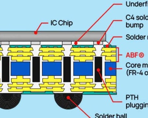
A glass substrate is a thin, high-precision sheet of engineered glass used as the base material for electronic devices. Unlike traditional FR4 or ABF substrates, glass provides an ultra-flat, chemically stable, and electrically insulating platform.

Typical glass substrate thickness ranges from:

  • 50 μm
  • 100 μm
  • 200 μm
  • 300 μm
  • 500 μm
  • 700 μm

The thickness depends on the final application, such as semiconductor packaging, display panels, or optical components.

Why Glass Substrates Are Becoming Popular

The demand for glass substrates is driven by several advantages over conventional organic materials.

Excellent Dimensional Stability

Glass experiences minimal thermal expansion during processing, enabling extremely accurate circuit alignment.

Superior Surface Flatness

Ultra-flat surfaces improve photolithography accuracy and support fine-line circuit fabrication.

Low Dielectric Loss

Glass offers excellent signal integrity for:

  • AI processors
  • High-speed networking
  • RF devices
  • High-frequency communication

High Thermal Stability

Glass can withstand elevated manufacturing temperatures without deformation.

Excellent Chemical Resistance

Glass substrates maintain structural integrity during wet chemical processing.

Common Materials Used in Glass Substrate Manufacturing

Several specialized glass materials are commonly used depending on the application.

Material Features Applications
Borosilicate Glass Low thermal expansion Semiconductor packaging
Aluminosilicate Glass High mechanical strength Mobile devices
Fused Silica Ultra-low dielectric loss Optical systems
Quartz Glass Excellent thermal resistance High-end electronics
Display Glass High transparency LCD & OLED displays

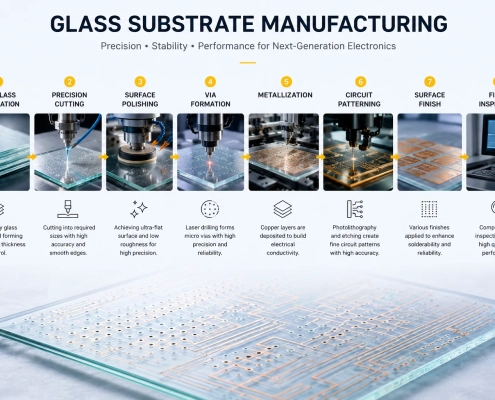
Glass Substrate Manufacturing Process

The manufacturing process requires extremely high precision to ensure flatness, dimensional accuracy, and electrical performance.

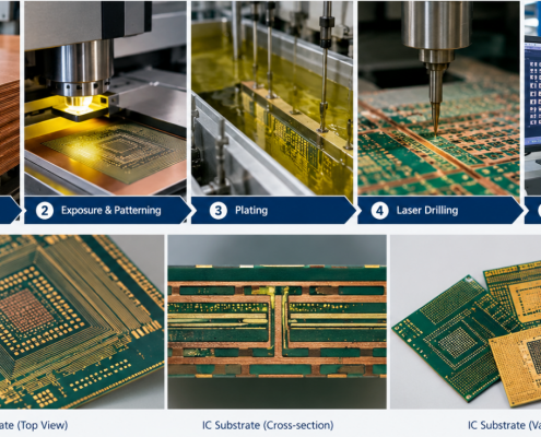
1. Raw Glass Preparation

High-purity glass is melted and formed into large panels with tightly controlled thickness.

Quality control focuses on:

  • Thickness tolerance
  • Surface roughness
  • Internal stress
  • Optical uniformity

2. Precision Cutting

Large glass panels are cut into customer-specific dimensions using:

  • Laser cutting
  • Diamond wheel cutting
  • CNC processing

Edge quality is critical to reduce cracking during subsequent processing.

3. Surface Polishing

Double-sided polishing removes microscopic surface defects and achieves nanometer-level flatness.

Benefits include:

  • Better lithography accuracy
  • Improved metal adhesion
  • Reduced particle contamination

4. Via Formation

Micro vias are created using:

  • Laser drilling
  • Wet etching
  • Dry plasma etching

Modern glass substrates can achieve via diameters below 20 μm.

5. Metallization

Copper conductive layers are deposited through processes such as:

  • Sputtering
  • Seed layer deposition
  • Electroplating

These conductive layers enable electrical interconnection.

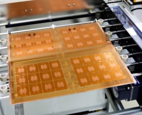
6. Circuit Patterning

Advanced photolithography transfers fine circuit patterns onto the substrate.

Current manufacturing capability can achieve:

  • Line/Space:
    • 5/5 μm
    • 3/3 μm
    • Even finer for advanced packaging

7. Surface Finish

Various surface finishes are applied according to customer requirements.

Common finishes include:

  • ENIG
  • ENEPIG
  • OSP
  • Immersion Silver

8. Final Inspection

Each substrate undergoes comprehensive quality inspection, including:

  • AOI inspection
  • Surface flatness measurement
  • Electrical testing
  • Thickness measurement
  • X-ray inspection
  • Reliability testing

Key Technologies in Glass Substrate Manufacturing

Modern manufacturing incorporates numerous advanced technologies.

Laser Micro Processing

Enables ultra-small via drilling with high positional accuracy.

Thin Glass Handling

Specialized automation prevents breakage during production.

Copper Metallization

Uniform copper deposition is essential for reliable electrical performance.

Fine-Line Lithography

Supports extremely dense semiconductor routing.

Cleanroom Manufacturing

Production typically occurs in ISO Class 5–7 cleanroom environments.

Applications of Glass Substrates

Glass substrates are used across multiple high-growth industries.

Semiconductor Advanced Packaging

Including:

  • 2.5D packaging
  • 3D IC
  • Chiplet architecture
  • AI processors

High-Performance Computing

Ideal for:

  • GPUs
  • AI accelerators
  • Data center processors

Display Industry

Widely used in:

  • LCD panels
  • OLED displays
  • Mini-LED
  • Micro-LED

Optical Components

Suitable for:

  • Camera modules
  • AR/VR devices
  • Optical sensors

Automotive Electronics

Including:

  • ADAS
  • Radar modules
  • Autonomous driving systems

Challenges in Glass Substrate Manufacturing

Although promising, manufacturing glass substrates presents several technical challenges.

Glass Brittleness

Thin glass is susceptible to cracking and requires specialized handling.

High Equipment Investment

Precision processing equipment significantly increases capital costs.

Complex Via Formation

Microvia fabrication is more challenging than PCB drilling.

Yield Optimization

Maintaining high production yield requires strict process control.

Future Trends

Industry analysts expect glass substrates to play an increasingly important role as semiconductor packaging advances.

Key trends include:

  • Larger panel sizes
  • Ultra-thin glass below 100 μm
  • Higher interconnect density
  • AI chip packaging
  • Chiplet integration
  • Co-packaged optics
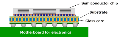
  • Glass core substrates for next-generation processors

Major semiconductor manufacturers are actively investing in glass substrate technologies to improve package performance while reducing signal loss and power consumption.

Choosing the Right Glass Substrate Manufacturer

When selecting a manufacturing partner, consider the following capabilities:

  • Advanced cleanroom facilities
  • Laser via drilling expertise
  • Fine-line circuit manufacturing
  • High-precision inspection systems
  • Semiconductor packaging experience
  • ISO-certified quality management
  • Custom engineering support
  • Stable high-volume production capacity

An experienced manufacturer can significantly improve product reliability while shortening development cycles.

Frequently Asked Questions (FAQ)

What is glass substrate manufacturing?

Glass substrate manufacturing is the process of producing precision-engineered glass panels for semiconductor packaging, displays, and advanced electronic applications through cutting, polishing, via formation, metallization, and circuit patterning.

Why are glass substrates replacing organic substrates?

Glass substrates offer lower thermal expansion, better flatness, lower dielectric loss, and improved dimensional stability, making them suitable for advanced semiconductor packaging.

Which industries use glass substrates?

Glass substrates are widely used in semiconductor packaging, AI computing, high-speed networking, OLED displays, automotive electronics, and optical devices.

What materials are used to manufacture glass substrates?

Common materials include borosilicate glass, aluminosilicate glass, fused silica, quartz glass, and specialty display glass.

Can glass substrates support fine-line circuitry?

Yes. Modern manufacturing technologies can achieve line widths below 5 μm, making glass substrates ideal for advanced chip packaging.

Conclusion

Glass substrate manufacturing is reshaping the future of semiconductor packaging and high-performance electronics. With exceptional electrical performance, superior dimensional stability, and compatibility with advanced fabrication technologies, glass substrates are poised to become a cornerstone material for AI, chiplets, and next-generation computing.

As demand for finer interconnects and more reliable packaging grows, partnering with an experienced glass substrate manufacturer ensures access to cutting-edge processes, stringent quality control, and scalable production capabilities.

FCBGA ABF substrate

We are a professional Flip-chip BGA substrate manufacturer. We can produce various types of substrates,  Ranging from 2 layers to 26 layers, and using ABF materials, Glass materials, Ceramic materials, BT materials, high-frequency materials, etc. Fast delivery, stable quality and reasonable price. If you have any design or production detail questions, you can contact us by email at any time and we are always ready to offer assistance. please send email to : PCB@ALCANTAPCB.COM

Semiconductor packaging is a crucial process in modern electronics, ensuring that integrated circuits (ICs) are securely connected to external systems while maintaining high performance and reliability. As electronic devices become smaller and more powerful, the choice of substrate material becomes critical, as it directly impacts heat dissipation, signal integrity, and electrical functionality. The FCBGA ABF substrate has emerged as a key solution in the industry, combining the high-density interconnection and thermal management benefits of FCBGA (Flip Chip Ball Grid Array) with the superior electrical performance and miniaturization capabilities of ABF (Ajinomoto Build-up Film). This powerful combination allows the FCBGA ABF substrate to meet the ever-growing demands of advanced electronic devices in sectors such as AI, telecommunications, and automotive technologies, making it an essential component in the future of semiconductor packaging.

阅读更多

absolics glass substrate

In the semiconductor industry, glass substrates are emerging as a next-generation material for advanced packaging and interconnects, offering advantages over traditional materials like silicon and ceramics. With superior properties such as higher thermal conductivity, better electrical insulation, and enhanced dimensional stability, glass substrates are ideal for high-performance applications, particularly in miniaturized and complex IC designs driven by chiplet technologies. Absolics stands at the forefront of this innovation, pioneering the development and manufacturing of glass substrates that enable improved performance and scalability in semiconductor packaging. Through cutting-edge technology and strategic collaborations, Absolics has established itself as a leader in the field, making Absolics glass substrate a crucial component in the next generation of electronic devices and systems.

阅读更多

glass core substrate

A Glass Core Substrate is an advanced material used in semiconductor packaging, designed to replace traditional organic substrates. Made from specialized glass, these substrates offer superior thermal resistance, mechanical stability, and low signal loss compared to organic materials like FR4 or BT. Glass core substrates are essential for high-performance applications such as 3D packaging, high-density interconnect (HDI) circuits, and next-generation IC packaging. They enable miniaturization and faster interconnects, supporting the demands of modern technologies like AI, 5G, and high-performance computing. Companies like Intel and TSMC are actively developing glass core substrates for future semiconductor packaging solutions. While they promise significant performance improvements, the manufacturing process is complex and costly, making widespread adoption challenging in the short term. However, as technology advances, glass core substrates are expected to play a key role in the evolution of semiconductor packaging, offering a more efficient and durable solution for high-end electronics.

阅读更多

bt substrate material

Substrate materials form the foundation of electronic manufacturing, providing structural support and electrical connections for components. Among these materials, bismaleimide triazine (BT) substrate stands out for its exceptional properties and widespread use in PCB manufacturing. Engineered from bismaleimide triazine resin, BT substrate material offers remarkable thermal stability, mechanical strength, and electrical performance, making it indispensable for high-performance electronic devices. Its significance lies in its ability to withstand harsh operating conditions, ensuring the reliability and longevity of electronic products. In this guide, we delve deeper into the world of BT substrate material, exploring its composition, applications, and manufacturing processes.

阅读更多