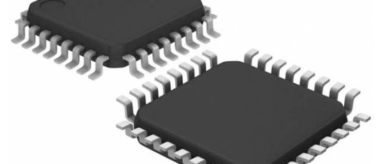
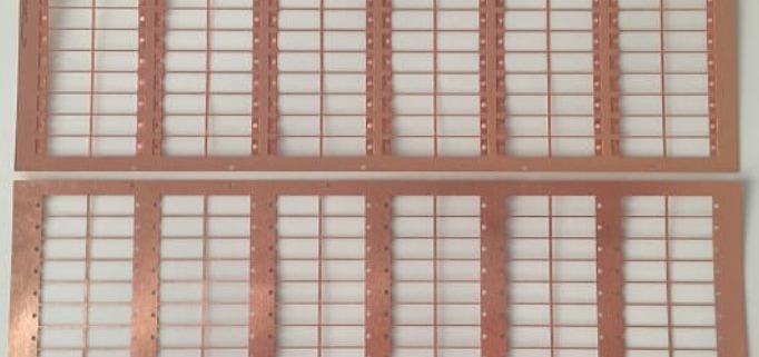
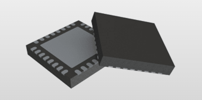
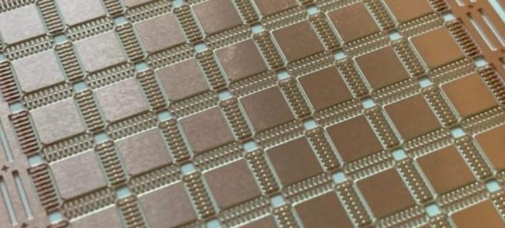
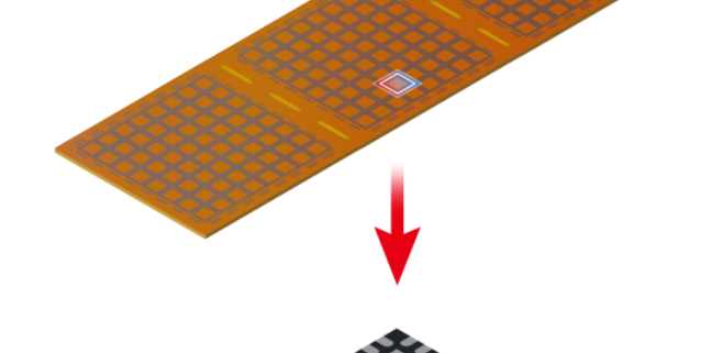
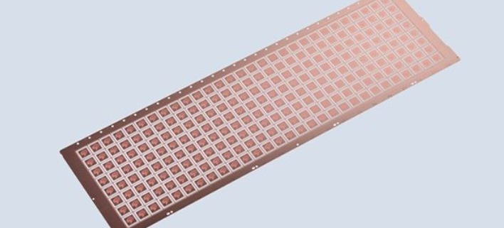
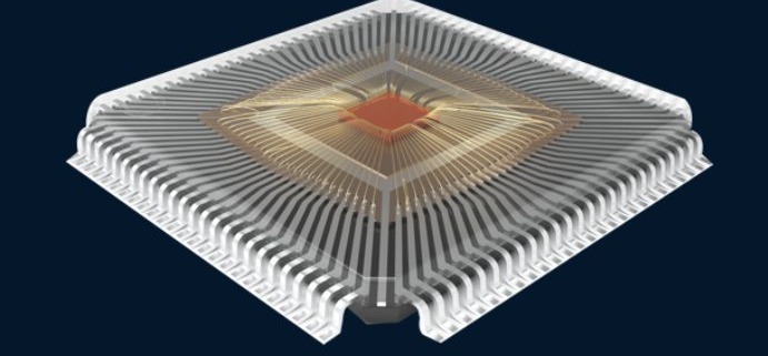
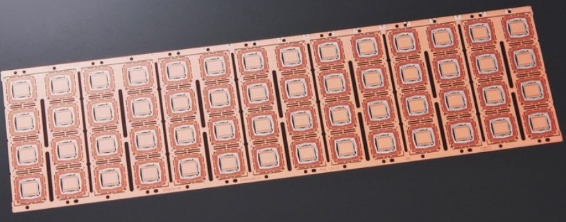
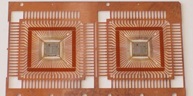
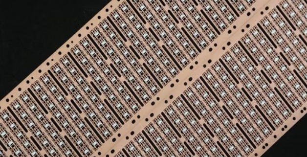
Quad Flat Pack Lead Frame

Semiconductor packaging is crucial in electronics, as it protects and connects integrated circuits (ICs), enabling them to function properly within devices. Packaging shields ICs from environmental factors like moisture and heat, while providing electrical connections to the external system. As electronic devices evolve, the demand for advanced packaging solutions increases. One such solution is the Quad Flat Pack Lead Frame, a popular packaging type that features a flat, rectangular shape with leads extending from all four sides. Lead frames are vital in many semiconductor packages, ensuring precise and reliable interconnects for a variety of applications. They support the IC during assembly, ensuring its functionality and longevity in end devices, making them an essential part of modern electronics.

阅读更多

Lead Frames Material C-194 F.H.

Lead frames are essential components in semiconductor device assembly, providing the metal base that supports and electrically connects the integrated circuit (IC) to the external circuitry. They act as a bridge between the chip and the package, ensuring proper electrical paths for signals and heat dissipation. The role of lead frames in electronic devices is crucial, as they enable effective power delivery and data transmission, allowing the IC to function within the system. In packaging technology, Lead Frames Material C-194 F.H. plays a central role due to its superior electrical and thermal properties, which meet the high demands of modern electronic applications. C-194 F.H. material ensures lead frames provide durability, efficiency, and reliability in high-performance environments.

阅读更多

Leadframes DFN

In the semiconductor industry, packaging plays a crucial role in protecting integrated circuits (ICs) and ensuring their functionality within electronic systems. Proper packaging not only safeguards the delicate ICs but also facilitates their integration with other components. One essential part of semiconductor packaging is the Leadframes DFN, which serves as the foundation for the connections between the chip and external devices. Leadframes are metal structures that help guide electrical signals from the IC to the board, offering both mechanical support and electrical conductivity. Among various packaging options, the DFN (Dual Flat No-lead) and QFN (Quad Flat No-lead) packages have gained significant popularity due to their compact size, high performance, and improved thermal dissipation. These packaging types, made possible by advanced leadframe technology, are commonly used in consumer electronics, automotive, and telecommunications, where space and reliability are paramount.

阅读更多

Copper Leadframe Substrate

A Leadframe is a crucial element in semiconductor packaging, providing the physical structure that holds and connects the semiconductor chip to external electrical contacts, while also enabling the transfer of signals and power. Over time, leadframes have evolved from basic designs to more complex forms, supporting the growing demands of miniaturized and high-performance electronic devices. A Substrate, on the other hand, serves as the supporting base for the chip, offering mechanical stability and facilitating electrical connections to the leadframe. While the leadframe focuses on structural integrity and electrical paths, the substrate also aids in heat dissipation. Copper, chosen for its superior thermal conductivity and electrical conductivity, plays a key role in leadframe technology. The Copper Leadframe Substrate combines these unique properties, ensuring efficient performance and enhanced reliability in semiconductor packaging.

阅读更多

Ultrathin QFN Lead Frame

In the world of modern electronics, packaging technology plays a crucial role in ensuring the performance, reliability, and miniaturization of electronic components. Lead frames, which are metal frameworks used to connect integrated circuits (ICs) to a printed circuit board (PCB), are a key component in this technology. Among various package types, the QFN (Quad Flat No-lead) package has become increasingly popular due to its compact size, low profile, and enhanced thermal performance. This design eliminates traditional leads, relying instead on solder pads underneath the package for connections. Recently, the demand for even more compact and efficient solutions has given rise to the trend of Ultrathin QFN Lead Frame. This innovation focuses on reducing the overall height of the QFN package while maintaining or improving thermal dissipation and electrical performance. Ultrathin QFN lead frames are particularly well-suited for applications requiring space-saving, such as mobile devices, wearables, and high-density electronics.

阅读更多

QFN Metal Lead Frame

QFN (Quad Flat No-lead) packaging is a popular and versatile surface-mount technology used to house integrated circuits (ICs). Unlike traditional leaded packages, QFN features flat, no-lead connections underneath the package, allowing for a smaller footprint and improved electrical performance. Central to the QFN package is the QFN Metal Lead Frame, which provides structural support, thermal management, and electrical connections between the chip and the PCB. The metal lead frame in QFN packages plays a critical role in the overall reliability and performance of the device, ensuring efficient heat dissipation and high-speed signal transmission.

QFN packaging is widely used in various modern electronic applications, including mobile devices, automotive systems, and consumer electronics. Its compact size, cost-effectiveness, and excellent thermal performance make it ideal for high-density, high-performance circuits, which are increasingly demanded in today’s advanced technologies. The QFN Metal Lead Frame thus serves as the foundation of this package, enabling the success of these applications.

阅读更多

QFN/QFP Lead Frame

Integrated Circuit (IC) packaging is a crucial aspect of PCB (Printed Circuit Board) design, as it directly impacts the performance, reliability, and size of electronic devices. Different IC packages are designed to meet the diverse requirements of modern electronics, ranging from compact mobile devices to high-performance computing systems. Among the various packaging options, QFN/QFP Lead Frame packages have become increasingly popular due to their unique design features and advantages.

Understanding the differences between these two packages—QFN (Quad Flat No-lead) and QFP (Quad Flat Package)—is essential for engineers and designers. Both packages offer distinct electrical, mechanical, and thermal properties, making them suitable for different applications. This article will delve into the key differences, applications, and advantages of QFN/QFP Lead Frame packages, helping readers make informed decisions about which package best suits their design needs.

阅读更多

QFN Lead Frame

In the world of modern electronics, packaging plays a critical role in ensuring the reliability, performance, and miniaturization of electronic devices. Effective packaging protects sensitive components from environmental factors while enabling efficient heat dissipation and electrical connections. Among the various packaging solutions, QFN (Quad Flat No-lead) packages have become a preferred choice due to their compact design, excellent thermal management, and superior electrical performance. The QFN Lead Frame is at the heart of this packaging technology, providing both structural support and electrical connectivity for the integrated circuit (IC) inside. This innovative lead frame design eliminates traditional leads, allowing for a more space-efficient layout, while also ensuring a high level of performance. As the demand for smaller, faster, and more efficient devices grows, the QFN Lead Frame continues to play a crucial role in advancing the capabilities of modern electronics.

阅读更多

QFN Micro Lead Frame

The QFN (Quad Flat No-lead) package is a popular surface-mount package used in modern electronic devices. It features a flat, square design with no leads, making it ideal for compact applications where space and performance are crucial. The QFN package allows for excellent thermal management and electrical performance, which is why it is widely used in consumer electronics, automotive, and communication systems. One of the most significant advancements in QFN technology is the introduction of the QFN Micro Lead Frame, which enhances the package’s overall performance by minimizing the lead frame size, improving signal integrity, and reducing parasitic inductance and resistance. This makes it highly suitable for high-speed, high-frequency applications. The design also helps optimize the manufacturing process, enabling more precise and reliable packaging to meet the growing demand for miniaturized electronic components.

阅读更多

BGA/IC Substrate

In the world of electronics, substrates play a crucial role as the foundational layer that supports and connects various components within a device. A substrate serves not only as a physical support but also as a medium for electrical connections, ensuring the functionality and reliability of the final product. Among the different types of substrates, BGA/IC Substrate has emerged as an essential technology in the development of modern devices.

The BGA (Ball Grid Array) and IC (Integrated Circuit) substrates are integral in high-performance applications, such as smartphones, computers, and automotive systems. These substrates provide superior signal integrity, heat dissipation, and miniaturization, addressing the increasing demand for faster and more compact electronic products.

In the PCB (Printed Circuit Board) industry, BGA/IC substrates represent a critical evolution in packaging and interconnection technologies, facilitating the development of next-generation electronics with enhanced efficiency and reduced size. Their importance continues to grow as electronic devices become increasingly complex and powerful.

阅读更多