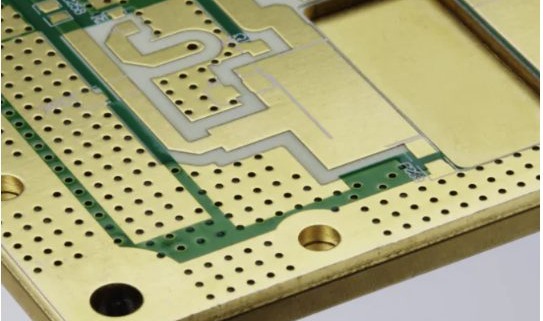
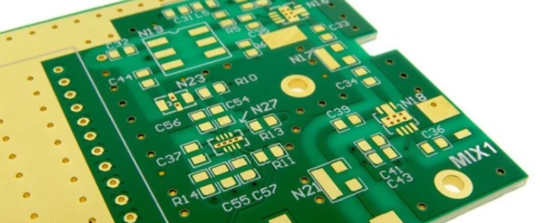
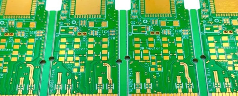
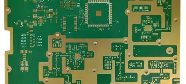
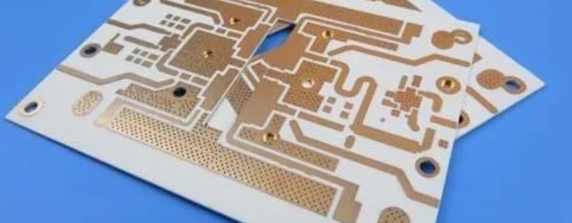
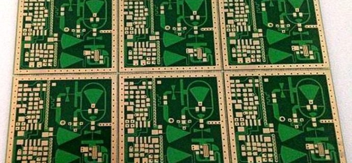
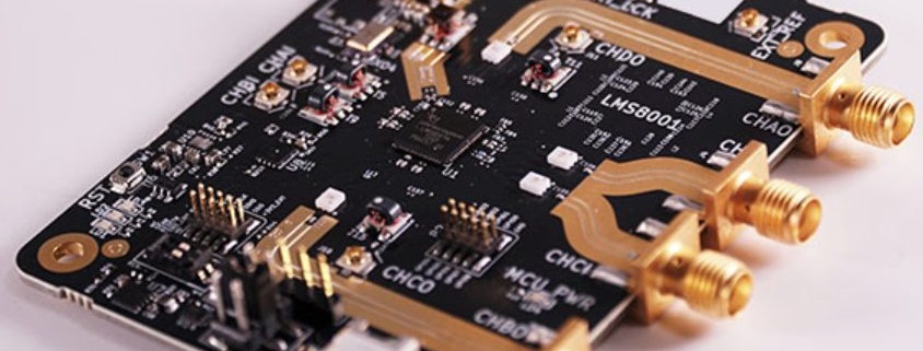
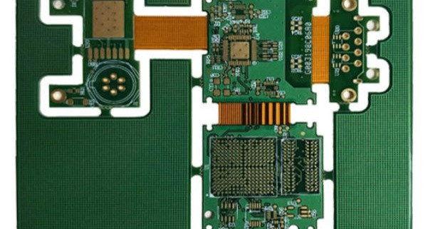
hdi pcb technology

HDI PCB technology, or High-Density Interconnect PCB technology, refers to a type of printed circuit board with a higher wiring density per unit area compared to conventional PCBs. It utilizes advanced design features such as laser-drilled microvias, blind and buried vias, and high-performance thin materials to achieve superior electrical performance and space efficiency.

The importance of high-density interconnect technology in modern electronics is significant, as it enables the development of compact, lightweight, and high-performance devices. This technology is widely used in smartphones, tablets, medical devices, aerospace systems, and automotive electronics, where miniaturization and reliability are crucial. By reducing signal loss and improving power distribution, it enhances device efficiency and functionality. As the demand for smaller and more powerful electronic products grows, this technology continues to be a key enabler of innovation in the electronics industry.

阅读更多

hdi pcb fabrication

HDI PCB (High-Density Interconnect PCB) is a cutting-edge printed circuit board technology that enhances circuit density by utilizing microvias, fine lines, and advanced lamination techniques. HDI PCB fabrication enables the design of compact, lightweight, and high-performance electronic devices, making it essential in modern technology.

The importance of HDI PCB fabrication lies in its widespread applications across industries such as consumer electronics, telecommunications, automotive, aerospace, and medical devices. Smartphones, tablets, wearables, and high-speed communication systems all rely on HDI PCBs to achieve miniaturization and improved signal integrity.

Compared to traditional PCBs, HDI PCBs offer several advantages, including higher electrical performance, reduced signal loss, and enhanced thermal management. The use of stacked and staggered vias improves reliability and increases layer interconnect density. Additionally, HDI PCB fabrication reduces the overall footprint of electronic products, making it a preferred choice for manufacturers aiming to optimize space and performance in modern circuit designs.

阅读更多

embedded cavity pcb manufacturing-1

Embedded Cavity PCB Manufacturing is an advanced process that integrates components within recessed cavities in the PCB structure, enabling reduced board thickness, improved electrical performance, and better thermal management. As electronic devices continue to shrink while requiring higher functionality, embedded cavity PCBs have become a key solution in modern electronics.

We have produced Embedded Cavity PCB boards using cutting-edge technology, ensuring precise depth control and high-accuracy cavity sizes. Our capabilities range from 4-layer to 30-layer designs, meeting diverse application needs. By embedding components directly into the PCB, this technology enhances miniaturization, reliability, and performance, making it ideal for high-frequency, high-power, and mission-critical applications. Embedded Cavity PCB Manufacturing offers superior electromagnetic shielding, shorter interconnects, and improved mechanical stability.

阅读更多

hdi pcb design

HDI PCB Design (High-Density Interconnect PCB) refers to advanced printed circuit boards with higher wiring density per unit area compared to traditional PCBs. High-density interconnect PCBs incorporate microvias, blind vias, and buried vias, allowing more compact circuit layouts and reducing the number of PCB layers. This technology supports miniaturization while enhancing signal integrity and performance. Compared to traditional boards, this design offers a significant advantage in terms of space optimization and lightweight construction, making it ideal for high-speed and high-frequency applications. Modern electronic devices such as smartphones, medical devices, and automotive systems heavily rely on this advanced design to achieve smaller form factors, faster signal transmission, and improved reliability. As demand for compact and efficient electronics rises, this technology continues to play a pivotal role in advancing innovation and meeting industry needs. 阅读更多

There are two main types of cavity PCB designs: open cavities and buried cavities. Open cavities involve creating single or multiple voids directly on the board’s surface. In contrast, buried cavities are positioned between inner layers, nestled within the PCB stackup. Both designs are feasible across a wide range of layer counts, from 4 layers up to 50 layers.

阅读更多

hdi flex pcb

HDI Flex PCBs (High-Density Interconnector Flexible Printed Circuit Boards) are advanced circuit boards that combine high-density interconnection (HDI) technology with the flexibility of traditional flexible PCBs. HDI technology enables the creation of circuits with finer traces, microvias, and stacked vias, which are essential for compact, high-performance designs. The flexibility of these PCBs makes them ideal for applications that require space and weight savings. In the modern electronics industry, HDI Flex PCB are crucial for the miniaturization and functionality of devices. They are widely used in industries such as medical devices, where compact and reliable designs are necessary; automotive, where space-saving and durable circuits are needed for advanced control systems; consumer electronics, especially in smartphones and wearables; and aerospace, where performance and flexibility under extreme conditions are vital. HDI Flex PCBs are a key technology enabling innovation across these sectors.

阅读更多

hdi pcb manufacturer

High-Density Interconnect (HDI) PCBs are advanced circuit boards that feature finer lines, smaller vias, and higher wiring density, enabling more complex and compact designs. As a critical component in modern electronics, HDI PCBs enhance signal integrity and reduce electromagnetic interference, making them ideal for high-performance applications such as smartphones, automotive systems, and medical devices. Compared to traditional PCBs, HDI PCBs employ microvias, blind and buried vias, and laser drilling technology, which significantly increases layer density and aspect ratio capabilities. While standard PCBs rely on through-hole vias and thicker traces, HDI PCBs achieve superior electrical performance through reduced signal loss and improved impedance control. As demand for miniaturization and high-speed applications continues to grow, selecting the right hdi pcb manufacturer becomes essential for ensuring quality and reliability in advanced electronics. 阅读更多

hdi pcb board

Printed Circuit Board (PCB) technology has evolved significantly over the years, transitioning from basic single-layer boards to complex multi-layer designs capable of supporting high-speed applications. Among these advancements, the HDI PCB board (High-Density Interconnect PCB) has emerged as a critical innovation, enabling the miniaturization of modern electronic devices. An HDI PCB board utilizes microvias, blind vias, and buried vias to achieve higher wiring density and reduce the overall footprint of the PCB. This allows for more compact designs while maintaining superior electrical performance. In today’s advanced electronics, such as smartphones, wearables, and automotive systems, the HDI PCB board plays a vital role by enhancing signal integrity, reducing electromagnetic interference (EMI), and supporting higher-frequency signals. Its ability to increase circuit density and optimize electrical characteristics makes the HDI PCB board indispensable for high-performance, space-constrained applications across various industries. 阅读更多

integrated press hole rogers pcb

Printed Circuit Boards (PCBs) are essential in modern electronics, providing the physical structure to connect electronic components and ensuring reliable electrical signals in devices like smartphones, computers, and medical equipment. Among the various types, Rogers PCBs are renowned for their superior performance in high-frequency applications, offering low signal loss, excellent thermal stability, and high electrical reliability. These attributes make them ideal for demanding fields like RF communication, radar systems, and satellite technology. An advanced variation, the Integrated Press Hole Rogers PCB, combines traditional drilling with an integrated press hole process, enhancing both manufacturing efficiency and electrical performance. This technology is particularly valuable in specialized applications, such as 5G networks, high-speed communications, and automotive radar systems, where high-frequency signal integrity and thermal management are crucial.

阅读更多

high speed press hole rogers pcb

High-speed press hole Rogers PCB refers to a specialized printed circuit board that utilizes Rogers Corporation’s high-frequency laminate materials combined with advanced press hole technology to maintain signal integrity in high-speed applications. Rogers PCB materials, such as RO4003C, RO5880 LZ, and RO3003, are known for their low dielectric loss, high thermal stability, and superior frequency performance, making them ideal for RF and microwave applications. Press hole technology involves precisely drilled holes that facilitate electrical and mechanical connections while minimizing parasitic effects. In high-speed circuits, press holes play a critical role in reducing signal reflections, maintaining impedance control, and ensuring reliable performance. The importance of high-speed press hole technology lies in its ability to enhance signal accuracy, reduce crosstalk, and minimize electromagnetic interference (EMI), making it indispensable for applications such as 5G communication systems, high-frequency radar, and aerospace electronics.

阅读更多