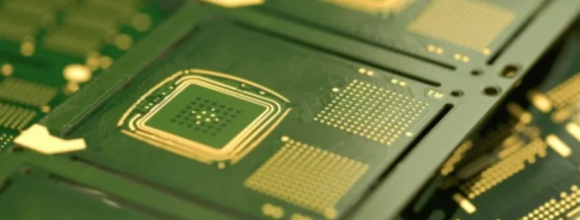
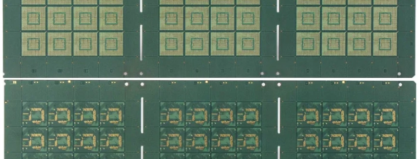
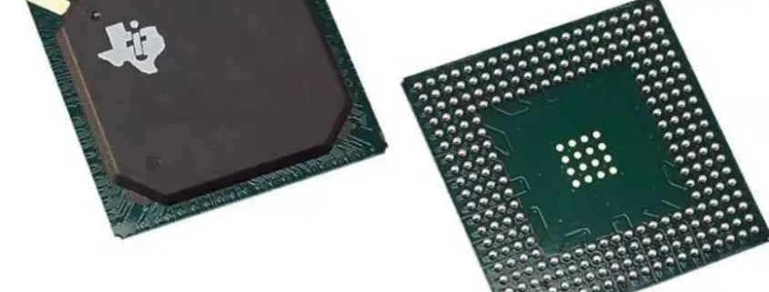
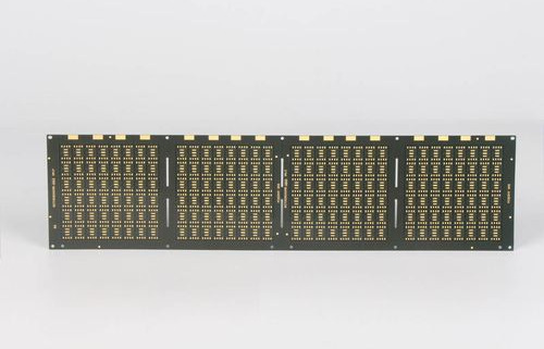
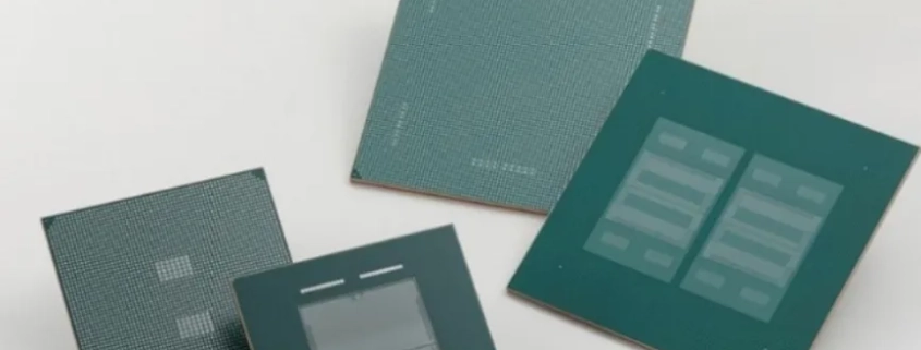
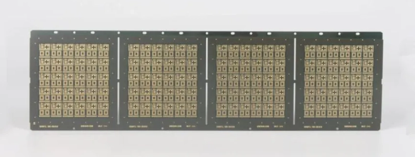
Ball Grid Array (BGA) technology has revolutionized electronics manufacturing with its compact design and high pin count capabilities. Widely adopted across various industries, BGAs provide efficient connectivity in devices ranging from smartphones to aerospace equipment. Central to the functionality of BGA packages is soldering, which ensures reliable electrical connections between the integrated circuits and the printed circuit board (PCB). However, despite their numerous advantages, BGA packages are susceptible to substrate cracks, presenting a significant concern in electronic assembly. Understanding the intricacies of BGA soldering and the potential risks associated with substrate cracks is crucial for ensuring the reliability and longevity of electronic products.
阅读更多Flip chip technology revolutionized electronic packaging by enabling smaller, faster, and more reliable devices. Unlike traditional wire bonding, flip chip bonding directly connects the chip to the substrate, enhancing electrical performance and reducing signal interference. This method finds extensive applications in microprocessors, memory chips, and high-speed communication devices. The substrate material in flip chip BGA packaging plays a crucial role in providing structural support, thermal dissipation, and electrical connectivity. Selecting the right substrate material ensures optimal performance, reliability, and manufacturability of flip chip BGA packages, making it a critical consideration in electronic design and manufacturing processes.
阅读更多BGA (Ball Grid Array) Substrate Materials are essential components in the packaging of modern electronic devices. They serve as the foundation for mounting integrated circuits (ICs) onto a PCB (Printed Circuit Board). The BGA Substrate Materials provide the necessary support for the solder balls that connect the chip to the board, ensuring reliable electrical and mechanical performance. These materials must meet strict requirements for thermal conductivity, electrical insulation, and mechanical strength to withstand the demanding conditions in high-performance electronics.
The significance of BGA Substrate Materials in modern electronic packaging cannot be overstated. As electronic devices continue to become smaller and more powerful, the need for efficient heat dissipation and robust signal transmission increases. BGA Substrate Materials are designed to meet these needs, offering superior performance in compact, high-density configurations. Their versatility makes them ideal for applications ranging from consumer electronics to automotive systems, where both performance and reliability are crucial.
In the ever-evolving landscape of electronics, Ball Grid Array (BGA) technology stands as a cornerstone of innovation. This compact and efficient packaging solution has revolutionized the way electronic components are interconnected, offering higher density and improved thermal performance. However, beneath the surface of BGA lies a crucial element often overlooked: substrate design. The substrate serves as the foundation for BGA, facilitating electrical connections while managing heat dissipation and ensuring signal integrity. Recognizing the pivotal role of substrate design is paramount, as it directly impacts the performance, reliability, and manufacturability of BGA-based systems. Thus, delving into the intricacies of BGA substrate design becomes imperative for engineers and designers striving to unleash the full potential of modern electronics.
阅读更多In today’s rapidly evolving electronics industry, the emergence of organic PCB substrate technology marks a significant milestone. This innovative approach not only revolutionizes traditional manufacturing processes but also underscores a crucial shift towards sustainability and performance. As the demand for environmentally friendly solutions continues to surge, organic PCB substrates have garnered immense attention for their unparalleled benefits. With their ability to deliver both high performance and eco-friendliness, these substrates are reshaping the landscape of PCB manufacturing. In this era of heightened environmental consciousness, the adoption of organic PCB substrates represents a proactive step towards reducing carbon footprint while ensuring optimal functionality in electronic devices.
阅读更多PCB substrate materials play a pivotal role in the functionality and reliability of modern electronics. As the backbone of printed circuit boards (PCBs), these materials serve as the foundation upon which electronic components are mounted and interconnected. The transition from older wiring methods to PCBs marked a significant advancement in electronic design and manufacturing. PCBs streamlined the assembly process, reduced production costs, and enhanced the overall performance of electronic devices. This evolution revolutionized various industries, from consumer electronics to aerospace, by enabling the creation of smaller, lighter, and more complex electronic systems. Understanding the importance and characteristics of PCB substrate materials is essential for engineers and designers striving to innovate in today’s rapidly evolving electronic landscape.
阅读更多Flexible PCBs (Flex PCBs) have revolutionized modern electronics with their versatility and adaptability to various applications. From smartphones to medical devices and aerospace technologies, Flex PCBs have become integral components due to their ability to conform to complex shapes and tight spaces.
In this article, we will delve into the fundamental aspects of Flexible PCB substrate materials, exploring their composition, characteristics, manufacturing processes, and application areas. By understanding the intricacies of Flex PCB materials, readers can gain insights into the crucial role they play in advancing electronic technologies. Whether you’re a seasoned engineer or a curious enthusiast, this comprehensive exploration will provide valuable insights into the backbone of modern electronic devices.
阅读更多Etchback in PCB manufacturing refers to the controlled removal of excess copper from the substrate surface, typically after the initial etching stage. This process ensures precise circuit patterns and optimal electrical performance. Substrate materials play a crucial role in PCB fabrication, providing the structural foundation and electrical insulation necessary for circuit integrity. The etchback process enhances the quality and reliability of PCBs by refining circuit geometry, minimizing signal distortion, and improving impedance control. Its significance lies in achieving tighter tolerances, reducing signal loss, and facilitating the integration of complex electronic components. Overall, etchback contributes to the production of high-performance PCBs vital for diverse applications in consumer electronics, telecommunications, aerospace, and beyond.
阅读更多Introducing the revolutionary Copper Clad Flexible PCB Substrate: a groundbreaking advancement poised to redefine the landscape of electronic circuitry. Engineered with precision and innovation, this cutting-edge substrate offers unparalleled flexibility and durability, transcending the limitations of traditional rigid PCBs. By seamlessly integrating flexibility with superior conductivity, it opens up a myriad of possibilities for designers and engineers, enabling the creation of intricately designed circuits in compact spaces. With its ability to withstand bending and flexing without compromising performance, this substrate empowers the development of next-generation electronic devices across industries, from consumer electronics to medical devices and beyond. Join us as we delve deeper into the transformative potential of Copper Clad Flexible PCB Substrates and their impact on the future of electronics.
阅读更多High-temperature PCB substrates play a pivotal role across diverse industries where reliability and performance are paramount. These substrates are engineered to withstand elevated temperatures, ensuring the integrity of electronic components in demanding environments such as automotive, aerospace, and industrial machinery. Central to understanding their efficacy is the concept of Tg, or glass transition temperature, which denotes the point at which the material transitions from a rigid to a more flexible state. In PCB materials, Tg signifies their ability to maintain structural integrity under heat stress, preventing warping, delamination, and electrical failure. As such, selecting substrates with an appropriate Tg is critical for ensuring the longevity and functionality of electronic devices operating in high-temperature conditions.
阅读更多CONTACT US
4th Floor, A3 Building, HuaFeng Industrial Park, GuanTian Village, BeiHuan Road, ShiYan Street, Bao An District, Shenzhen City, Guangdong Province, China
Tel:086 (0)755-8524-1496
WhatsApp: 8615014077679
Skype: Henrychinasz
📧 pcb@alcantapcb.com
CONTACT US
SHIPPING
CERTIFCATION
recent articles
- Small Outline Integrated Circuit(SOIC) in PCB Design2025-03-12 - 2:43 上午
- TSOP/LOC Lead Frame and Its Role in Semiconductor Packaging2025-03-11 - 2:38 上午
- Key Benefits of Plastic Leaded Chip Carrier (PLCC) Lead Frame2025-03-10 - 2:47 上午
- Advantages of Plastic Dual In-line Package(PDIP) Lead Frame2025-03-07 - 3:03 上午