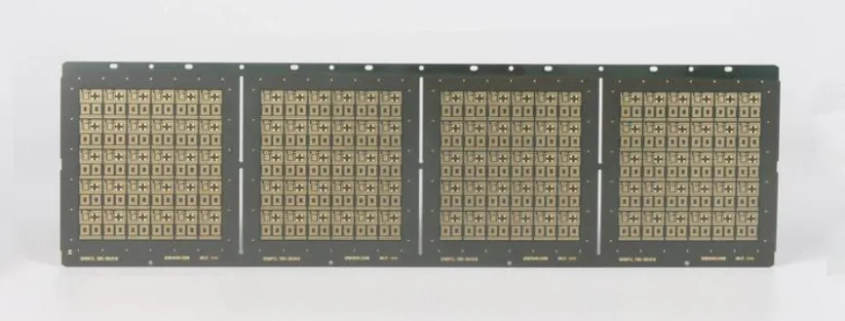
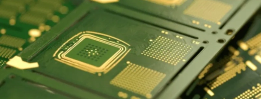
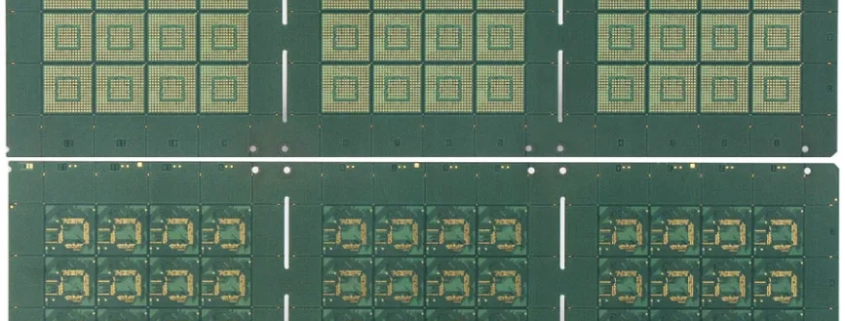
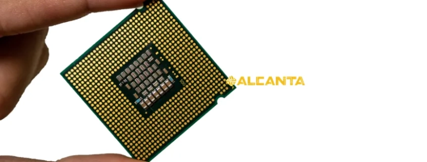
PCB Substrate serves as the foundation of a printed circuit board (PCB), providing mechanical support and electrical connectivity for electronic components. Its significance lies in ensuring the structural integrity of the PCB while facilitating the transmission of signals between components. Functionally, Substrate PCB acts as a dielectric material between copper traces, preventing short circuits and facilitating the flow of electrical signals across the board. Moreover, it influences the PCB’s thermal and electrical performance, affecting factors like signal integrity and reliability. Understanding the role of Substrate PCB is crucial in optimizing circuit board design for various applications, ensuring robust performance and longevity of electronic devices.
阅读更多Chip on Board (COB) technology revolutionizes traditional electronic packaging by directly mounting semiconductor chips onto a substrate. This method eliminates the need for individual packaging, leading to a compact, efficient design. COB has evolved from its inception in the late 20th century to become a cornerstone of modern electronics, offering significant advancements in miniaturization, performance, and reliability. Its application extends beyond electronics, particularly in LED lighting where COB configurations deliver unparalleled brightness and energy efficiency. Moreover, COB technology finds utility in various fields like automotive, medical devices, and consumer electronics, emphasizing its versatility and indispensability in contemporary engineering.
阅读更多Introducing emerging technological products is pivotal for steering technological advancements. In today’s digital landscape, the emergence of 3D IC Package Substrate stands as a testament to innovation in the electronics sector. This article embarks on an exploration of this groundbreaking technology, unraveling its intricacies and unveiling its myriad potential applications. From its inception to its current advancements, we’ll delve deep into the realm of 3D IC Package Substrate, shedding light on the transformative impact it promises to have on various industries. Join us on this journey as we uncover the fascinating world of 3D IC Package Substrate and its role in shaping the future of technology.
阅读更多In the dynamic landscape of the integrated circuit (IC) industry, chip carriers stand as indispensable components, serving as the bridge between the semiconductor chip and the broader electronic system. These carriers, in their various forms and configurations, play a pivotal role in enabling the functionality and performance of electronic devices we rely on daily. They facilitate the seamless integration of semiconductor chips into complex electronic systems, ensuring efficient signal transmission, thermal management, and mechanical support. As the demand for smaller, faster, and more powerful electronic devices continues to surge, the significance of chip carriers in enabling advancements in IC design and manufacturing cannot be overstated. From consumer electronics to industrial applications, chip carriers form the backbone of modern electronic systems, driving innovation and pushing the boundaries of what’s possible in the realm of semiconductor technology.
阅读更多Surface Mount Devices (SMD) represent a ubiquitous form of component packaging integral to modern electronic devices. Unlike traditional through-hole components, SMDs are affixed directly onto the circuit board’s surface, eliminating the need for perforations. This streamlined mounting method not only conserves space but also enhances manufacturing efficiency and electrical performance. SMD technology has revolutionized the electronics industry, enabling the creation of increasingly compact and sophisticated devices. Its versatility and reliability have made it indispensable across various sectors, from consumer electronics to aerospace and beyond. Understanding the diverse types and applications of SMD packages is essential for engineers and enthusiasts navigating the intricate landscape of electronic design and production.
阅读更多In the realm of electronic components, showcasing performance is paramount. Surface mount diode packages play a pivotal role in ensuring optimal functionality and efficiency in various electronic devices. This blog aims to delve into the intricacies of surface mount diode packages, shedding light on their diverse types, advantages, and applications. By understanding the nuances of these components, readers can grasp their significance in modern electronics and appreciate how they contribute to the seamless operation of devices we rely on daily. From exploring common package types to highlighting their unique features, this overview sets the stage for an insightful exploration into the world of surface mount diode packages.
阅读更多Chip on Board (COB) lighting represents a revolutionary approach to LED technology. Unlike traditional LEDs where individual diodes are mounted onto a substrate, COB integrates multiple LED chips directly onto a single substrate. This compact arrangement eliminates the need for individual LED packages, reducing size and improving thermal management. The working principle involves bonding LED chips directly onto a circuit board, enabling higher packing densities and enhanced light output. COB LEDs deliver several advantages, including improved energy efficiency, higher brightness, and better color rendering. Additionally, their compact size and simplified design make them ideal for various lighting applications, from residential to industrial settings. Overall, COB lighting stands out for its innovative design and superior performance in delivering efficient and high-quality illumination.
阅读更多In recent years, LED lighting has witnessed a remarkable surge in popularity, becoming the go-to choice for energy-efficient and eco-friendly illumination solutions. This trend stems from the increasing awareness of environmental sustainability and the pressing need to reduce energy consumption worldwide. Amidst this landscape, Chip on Board (COB) LED technology has emerged as a pioneering advancement, offering unparalleled advantages in brightness, integration, and thermal management. In this blog, we delve into the rise of COB LED technology, exploring its innovative features and comparing them with traditional LED counterparts. Join us as we unravel the intricacies of COB LED and its transformative impact on the lighting industry.
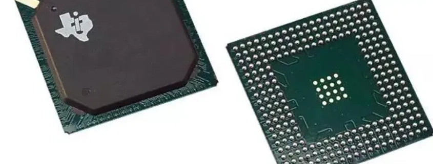
阅读更多Integrated circuit (IC) packages are critical components in modern electronics, protecting delicate IC chips, facilitating connections, and ensuring efficient thermal management. There are many different types of IC packages, each designed to meet specific requirements in terms of performance, size, and cost. Common types include DIP (dual in-line package) for simplicity, SMD packages such as SOP and QFP for compact designs, and BGA (ball grid array) and CSP (chip scale package) for high-density applications.
Introduction: Rogers Corporation, a leading global provider of advanced materials solutions, plays a pivotal role in the electronics industry. With a rich history of innovation, Rogers is renowned for its high-performance substrate materials, which are integral components in a wide array of modern electronic products. From telecommunications to aerospace, Rogers substrate materials are essential for enabling high-frequency signal transmission, thermal management, and reliability in electronic circuits. As electronic devices continue to evolve in complexity and functionality, the demand for Rogers substrate materials grows, reinforcing the company’s significance in driving technological advancements and shaping the future of electronics.
阅读更多CONTACT US
4th Floor, A3 Building, HuaFeng Industrial Park, GuanTian Village, BeiHuan Road, ShiYan Street, Bao An District, Shenzhen City, Guangdong Province, China
Tel:086 (0)755-8524-1496
WhatsApp: 8615014077679
Skype: Henrychinasz
📧 pcb@alcantapcb.com
CONTACT US
SHIPPING
![]()
CERTIFCATION
![]()
recent articles
 Copper Core PCB vs Aluminium Core PCB Explained2025-09-18 - 7:13 上午
 Microwave PCB Manufacturers | RF Design and Fabrication2025-09-16 - 7:58 上午
 Flex PCB Manufacturing Process: Step-by-Step Guide2025-09-10 - 6:59 上午
 PCB Lamination Process & Sequential Lamination2025-09-04 - 8:10 上午

