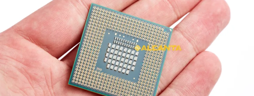
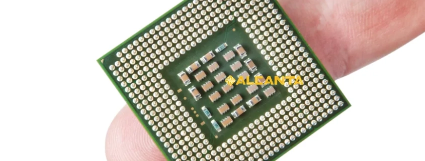
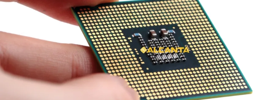
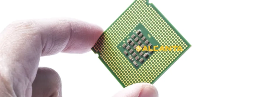
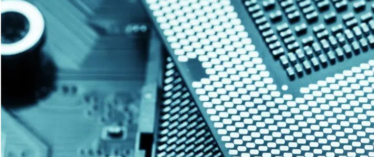
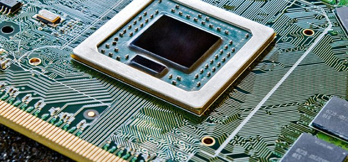
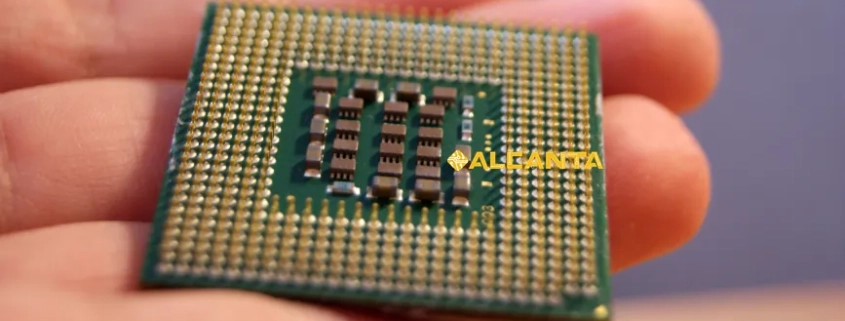
how to solder qfn package

Quad Flat No-leads (QFN) packages are a popular choice in modern electronics due to their compact size, excellent thermal performance, and reliable electrical connections. These packages feature a flat bottom surface with exposed pads for soldering, eliminating the need for traditional leads.

Proper soldering techniques for QFN packages are crucial for ensuring optimal functionality and reliability of electronic devices. The intricate design of QFN packages demands precision during soldering to prevent issues such as poor connections, solder bridges, or misalignment, which can lead to performance degradation or even device failure. In this guide, we will delve into the essential methods and tools required to master the art of soldering QFN packages effectively.

阅读更多
flip chip qfn package

In the rapidly evolving landscape of electronic packaging, understanding the fundamentals of QFN and Flip Chip packaging is essential. QFN packaging, known for its compact design and cost-effectiveness, contrasts with the sophisticated Flip Chip technology, renowned for its high performance and density. This article delves into the nuanced realm of packaging methodologies, with a specific focus on the innovative synthesis known as Flip Chip QFN Package. By exploring its unique amalgamation of QFN’s economic benefits and Flip Chip’s advanced features, we aim to unravel the unparalleled advantages and distinctive characteristics this packaging solution offers in the realm of electronic engineering.

阅读更多
fc qfn package

In the realm of electronics, packaging plays a pivotal role, acting as the interface between semiconductor devices and their environment. It ensures protection, thermal management, and electrical connections critical for device functionality. Among the modern packaging solutions, FC QFN (Flip Chip Quad Flat No-Lead) packages stand out for their innovative design and performance. These packages offer a compact, leadless structure, optimizing space utilization while enhancing thermal dissipation and electrical performance. As electronics continue to evolve, the importance of advanced packaging solutions like FC QFN becomes increasingly apparent, driving efficiency, reliability, and miniaturization in electronic devices.

阅读更多
dual row qfn package

Dual Row QFN (Quad Flat No-Lead) Package is a type of surface mount semiconductor package featuring a lead frame with leads on all four sides, arranged in two rows. Unlike traditional single row QFN packages, dual row QFNs offer increased lead counts and improved electrical performance. 

QFN packages, in general, have gained popularity due to their compact size, excellent thermal dissipation properties, and high electrical performance. They are widely used in various electronic applications where space-saving and efficient heat dissipation are critical factors. Now, let’s delve deeper into the specifics of dual row QFN packages and their unique advantages.

阅读更多
ceramic qfn package

In the fast-paced realm of electronics, packaging plays a pivotal role, dictating the efficiency, reliability, and miniaturization of devices. Among the array of packaging options, Quad Flat No-leads (QFN) packaging stands out for its significance and extensive utilization across the electronics industry. Its ability to facilitate compact designs, enhance thermal dissipation, and streamline manufacturing processes has made it a preferred choice for various applications. Within the QFN spectrum, Ceramic QFN Package emerges as a notable advancement, promising heightened performance in high-temperature, high-frequency, and high-power scenarios. This article delves into the concept and distinctive attributes of Ceramic QFN Package, exploring its pivotal role in shaping the future landscape of electronic devices.

阅读更多
ceramic qfn package

The Air Cavity QFN Package represents a groundbreaking evolution in semiconductor packaging, distinguished by its innovative design featuring a hollow cavity beneath the die. This design offers unparalleled thermal dissipation capabilities, crucial for high-power applications. Compared to conventional QFN packages, which lack this cavity, the air cavity QFN package boasts superior heat management, ensuring enhanced reliability and performance in demanding environments. This advancement addresses longstanding limitations in traditional QFN packages, making it a preferred choice for applications requiring efficient heat dissipation and reliability.

阅读更多
64 pin qfn package

In the realm of modern electronics, Quad Flat No-leads (QFN) packages have emerged as pivotal components, offering a blend of compactness, efficiency, and performance. These packages revolutionize circuit miniaturization and enhance thermal dissipation, critical in today’s compact electronic devices. Among the myriad QFN variants, the 64-pin QFN package stands out for its versatility and widespread utilization in diverse applications. This specific variant provides an optimal balance between pin count and form factor, making it a preferred choice for various integrated circuits and semiconductor devices. Understanding the intricacies of the 64-pin QFN package unveils insights into its crucial role in advancing electronic engineering.

阅读更多
48 pin qfn package

In the realm of modern electronics, the significance of Quad Flat No-leads (QFN) packages cannot be overstated. These compact, versatile packages have revolutionized circuit design and miniaturization, offering a compelling solution for a wide range of applications. By eliminating leads and utilizing a bottom-side connection design, QFN packages optimize space utilization, enhance thermal management, and improve electrical performance. Within this landscape, our blog zeroes in on a specific variant: the 48-pin QFN package. With its balanced pin count and strategic design, the 48-pin QFN presents an ideal choice for numerous electronic applications. Throughout this exploration, we delve into its intricacies, benefits, drawbacks, and the manufacturing processes that underpin its creation, offering insights crucial for engineers, designers, and enthusiasts alike. Join us as we uncover the inner workings and practical implications of this indispensable component in modern electronics.

阅读更多
32 qfn package

The 32 QFN Package represents a significant advancement in electronic packaging technology. Its compact size and versatility have revolutionized various industries, from consumer electronics to automotive and aerospace. Understanding its intricacies and advantages is crucial for engineers and designers striving for efficiency and performance in their products. By delving into the features and applications of the 32 QFN Package, we can uncover innovative solutions to complex design challenges and enhance the functionality of electronic devices. This exploration aims to shed light on the importance of embracing this packaging form and harnessing its potential for future advancements in technology and product development.

阅读更多
What Is ABF Substrate

What is ABF substrate? ABF substrate, short for Ajinomoto Build-Up Film substrate, is a crucial component in the semiconductor industry. Essentially, ABF substrate refers to a specialized material utilized in semiconductor packaging and interconnection processes. Its significance lies in its ability to provide high-density interconnects, enabling efficient communication between semiconductor components. ABF substrate plays a pivotal role in the development of advanced electronic devices, such as microprocessors and memory chips. Its unique properties make it suitable for various applications, including flip-chip packaging, multi-chip modules, and high-speed data transmission systems. Understanding what ABF substrate is and its applications is essential for grasping the complexities of modern semiconductor technology.

阅读更多