
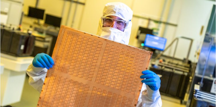
Advanced Materials for Efficiency: SLP Substrate Like PCB
Printed Circuit Boards (PCBs) are the backbone of most electronic devices, providing the necessary platform to connect and support electronic components. PCBs are composed of multiple layers of copper and insulating material laminated together. They offer a compact and efficient way to route electrical signals and power throughout a device, making them indispensable in the manufacture of everything from household electronics to advanced industrial machinery.
In recent years, a new advancement known as Substrate Like PCB (SLP) has emerged, gaining significant traction in modern electronic design. SLPs are an evolution of traditional PCBs, designed to meet the increasing demands for higher density and performance. They utilize advanced materials and manufacturing techniques to create finer circuit patterns, allowing for more compact and efficient designs. This innovation is particularly crucial for the latest generation of consumer electronics, such as smartphones and wearable devices, where space and performance are at a premium. The growing significance of SLP in the industry highlights its potential to push the boundaries of what is possible in electronic design.
Basic Differences Between PCB and SLP
Define PCB and its uses
Printed Circuit Boards (PCBs) are essential components in modern electronics, acting as the foundation for most electronic devices. They are constructed by laminating layers of copper and insulating material, such as fiberglass, to create a solid, flat board. The copper layers are etched to form conductive pathways that connect various electronic components, such as resistors, capacitors, and integrated circuits. PCBs provide a compact, efficient, and reliable way to interconnect these components, making them crucial in a wide range of applications, from simple household gadgets to complex industrial machinery and advanced computing systems.
Define SLP and its characteristics
Substrate Like PCBs (SLPs) represent a significant advancement over traditional PCBs. They are designed to meet the increasing demand for higher density and performance in modern electronic devices. SLPs are characterized by their finer circuit patterns and advanced materials, which enable more compact and efficient designs. The primary characteristics of SLPs include higher wiring density, reduced layer count, and improved electrical performance. These features are particularly advantageous for devices that require miniaturization and enhanced functionality, such as smartphones, tablets, and wearable technology.
Highlight the main differences between PCB and SLP
Structure and materials
Traditional PCBs are typically made from materials like FR4, a composite of woven fiberglass cloth with an epoxy resin binder. The structure involves multiple layers of copper and insulating materials laminated together. In contrast, SLPs use more advanced materials, such as high-density interconnect (HDI) substrates and finer pitch components. The structure of SLPs allows for thinner traces and smaller vias, leading to increased wiring density and better performance in a smaller footprint.
Manufacturing processes
The manufacturing process for traditional PCBs involves several steps, including layering, etching, drilling, and plating. These processes are relatively straightforward but can be limited in terms of the achievable density and precision. SLPs, on the other hand, utilize more advanced manufacturing techniques such as laser drilling for microvias, advanced etching processes, and high-precision lithography. These methods allow for the creation of much finer circuit patterns and more complex interconnections, resulting in higher performance and reliability.
Application scenarios
PCBs are widely used in a broad range of applications, from simple consumer electronics to complex industrial and military systems. They provide a reliable and cost-effective solution for general electronic needs. SLPs, due to their higher density and advanced performance characteristics, are particularly suited for applications where space and efficiency are critical. This includes high-end consumer electronics like smartphones and tablets, wearable devices, and advanced computing systems. The compact and efficient nature of SLPs makes them ideal for modern devices that require high performance in a small form factor.
While traditional PCBs remain a cornerstone of electronic device manufacturing, SLPs offer significant advancements in terms of density, performance, and miniaturization. The choice between PCB and SLP depends on the specific requirements of the application, with SLPs being the preferred option for high-density, high-performance designs.
Overview of SLP PCB
Composition and Structural Features of SLP PCB
Substrate Like PCBs (SLPs) are designed to meet the demands for miniaturization and enhanced performance in modern electronics. The composition of SLPs involves advanced materials and sophisticated manufacturing techniques. Typically, SLPs use high-density interconnect (HDI) substrates, which are made from materials like epoxy resin or polyimide, providing better mechanical and thermal properties compared to traditional FR4 materials. The structural features of SLPs include multiple layers with finer circuit patterns, microvias, and thinner traces, allowing for greater component density.
SLPs often incorporate advanced layering techniques, such as sequential build-up (SBU) technology, which allows for the creation of multiple, ultra-thin layers. This construction method is essential for achieving the high-density interconnects required in modern devices. Additionally, SLPs use laser-drilled microvias to connect these layers, significantly reducing the size of vias and enabling more compact designs.
Application of SLP PCB in High-Density Interconnect (HDI)
SLP PCBs are a critical component in High-Density Interconnect (HDI) technology, which is essential for producing high-performance electronic devices. HDI involves the use of finer lines and spaces, smaller vias, and higher connection pad density to create more complex and compact circuit designs. SLPs, with their advanced materials and manufacturing techniques, are well-suited for HDI applications.
In HDI designs, SLPs allow for the placement of more components in a smaller area, improving the overall performance and functionality of the device. This is particularly important in applications like smartphones, tablets, and wearable devices, where space is at a premium. The ability to create complex interconnects with high reliability makes SLPs an ideal choice for these high-performance applications.
Advantages of SLP PCB, Such as Higher Density and Performance
SLP PCBs offer several advantages over traditional PCBs, primarily in terms of density and performance. These advantages include:
- Higher Density: SLPs enable the creation of finer circuit patterns and smaller vias, allowing for a higher component density. This is crucial for modern electronic devices that require more functionality in a compact form factor.
- Enhanced Performance: The use of advanced materials and manufacturing processes in SLPs results in better electrical performance. This includes lower signal loss, higher signal integrity, and improved thermal management, which are essential for high-speed and high-frequency applications.
- Miniaturization: SLPs support the trend towards miniaturization in electronics, enabling the development of smaller, lighter, and more portable devices without compromising on functionality or performance.
- Improved Reliability: The advanced manufacturing techniques used in SLP production, such as laser-drilled microvias and sequential build-up layering, result in more robust and reliable connections. This is particularly important in applications where device failure is not an option, such as in medical devices and aerospace electronics.
- Design Flexibility: SLPs offer greater design flexibility, allowing engineers to create more complex and innovative designs. This flexibility is essential for developing next-generation electronic devices that push the boundaries of technology.
SLP PCBs represent a significant advancement in PCB technology, offering higher density, enhanced performance, and greater reliability. Their application in HDI and other high-performance electronic designs underscores their importance in the development of modern, compact, and high-functioning electronic devices.
Differences Between PCB and Substrate
Define What a Substrate Is
A substrate in the context of electronics and semiconductors is a base material upon which circuits are built. Substrates are typically composed of a flat, solid material that serves as a foundation for the various layers of conductive and insulating materials required to form electronic circuits. Common materials for substrates include silicon, ceramics, glass, and specialized polymers, each chosen for their specific mechanical, thermal, and electrical properties.
Differences Between Substrate and Traditional PCB
1. Material Composition:
- Traditional PCBs: These are primarily made from composite materials like FR4, which is a combination of woven fiberglass cloth with an epoxy resin binder. This material provides a good balance of strength, durability, and electrical insulation.
- Substrates: Substrates used in semiconductor manufacturing are often made from high-purity silicon or other advanced materials like gallium arsenide (GaAs) and silicon carbide (SiC). These materials are selected for their exceptional electrical properties and ability to support high-speed and high-frequency operations.
2. Structural Differences:
- Traditional PCBs: PCBs typically consist of multiple layers of copper and insulating material laminated together. The conductive layers are etched to form the required circuit patterns, and vias (holes) are drilled to create connections between layers.
- Substrates: Substrates are generally used as the base layer upon which semiconductor devices or integrated circuits (ICs) are fabricated. They may support single-layer or multi-layer constructions, often involving intricate processing techniques such as photolithography to create the necessary circuit patterns and microstructures.
3. Manufacturing Processes:
- Traditional PCBs: The manufacturing process for PCBs involves steps such as layering, etching, drilling, and plating. These processes are relatively straightforward and are suitable for creating a wide range of circuit board designs with varying complexities.
- Substrates: The manufacturing of substrates, especially for semiconductors, involves highly precise and complex processes. This includes wafer fabrication, doping, oxidation, photolithography, and etching. These steps are carried out in cleanroom environments to ensure the purity and precision required for semiconductor device performance.
4. Applications:
- Traditional PCBs: PCBs are used in a broad spectrum of applications, including consumer electronics (e.g., televisions, smartphones, computers), industrial equipment, automotive systems, and military devices. They provide a versatile and reliable platform for mounting and interconnecting electronic components.
- Substrates: Substrates are integral to the fabrication of semiconductor devices and integrated circuits (ICs). They are used in applications requiring high precision and performance, such as microprocessors, memory chips, sensors, and power devices. Substrates are also crucial in advanced technology applications, including telecommunications, aerospace, and medical devices.
Application of Substrate in Semiconductors and Integrated Circuits
Substrates play a critical role in the semiconductor industry, serving as the foundational layer for fabricating integrated circuits (ICs). In semiconductor manufacturing, the substrate (often a silicon wafer) undergoes a series of processing steps to create the desired electronic structures:
- Wafer Fabrication: High-purity silicon wafers are prepared as substrates, providing a flat and defect-free surface for circuit formation.
- Doping: Specific areas of the substrate are doped with impurities to modify their electrical properties, creating regions of n-type and p-type silicon essential for transistor function.
- Oxidation and Deposition: Thin layers of insulating materials, such as silicon dioxide, are grown or deposited on the substrate to isolate different regions of the circuit.
- Photolithography: This process uses light to transfer intricate circuit patterns onto the substrate, allowing for the precise creation of microstructures required for IC functionality.
- Etching and Deposition: Various etching techniques are used to remove unwanted material, while deposition processes add conductive or insulating layers, building up the complex architecture of the IC.
- Packaging: Finally, the completed semiconductor devices are cut from the substrate, packaged, and tested before being integrated into electronic systems.
The use of substrates in semiconductor and IC manufacturing enables the creation of highly complex and miniaturized electronic components, driving advancements in technology and performance across numerous industries.
Best Substrate Materials for PCB
Common PCB Substrate Materials
Several types of materials are commonly used as substrates for Printed Circuit Boards (PCBs), each offering unique properties suited to different application requirements:
- FR4 (Flame Retardant 4):
- Composition: Made from woven fiberglass cloth impregnated with an epoxy resin binder.
- Properties: Good electrical insulation, mechanical strength, and dimensional stability.
- Applications: Suitable for a wide range of electronic devices, from consumer electronics to industrial equipment.
- CEM-1 (Composite Epoxy Material 1):
- Composition: Similar to FR4 but with a lower fiberglass content and a different resin composition.
- Properties: Lower cost compared to FR4, but with reduced mechanical strength and dimensional stability.
- Applications: Used in simpler electronic applications where cost-effectiveness is prioritized over high performance.
- FR2:
- Composition: Made from paper impregnated with a phenolic resin.
- Properties: Low-cost option with moderate electrical and mechanical properties.
- Applications: Commonly used in single-layer PCBs for low-cost consumer electronics and toys.
- Aluminum-based PCBs:
- Composition: Metal core (usually aluminum) with a dielectric layer and copper foil.
- Properties: Excellent thermal conductivity, suitable for high-power LED lighting and automotive applications.
- Applications: Where heat dissipation is critical, such as LED drivers, power supplies, and automotive electronics.
Pros and Cons of Various Substrate Materials
- FR4:
- Pros: Good electrical insulation, mechanical strength, and widely available.
- Cons: Can be relatively heavy and may have limitations in high-frequency applications due to dielectric loss.
- CEM-1:
- Pros: Lower cost compared to FR4.
- Cons: Reduced mechanical strength and dimensional stability, less suitable for complex designs or high-performance applications.
- FR2:
- Pros: Low-cost option suitable for basic electronics.
- Cons: Limited mechanical and electrical properties, primarily used in single-layer applications.
- Aluminum-based PCBs:
- Pros: Excellent thermal conductivity, superior heat dissipation capabilities.
- Cons: Higher cost compared to traditional FR4 or CEM materials, limited flexibility in design compared to flexible PCBs.
Recommendations for Choosing the Best Substrate Material
Choosing the best substrate material depends on the specific requirements of the application:
- High-Frequency Applications:
- Recommended Materials: High-frequency laminates such as Rogers 4000 series or Teflon-based materials (PTFE).
- Reason: These materials offer low dielectric loss and consistent electrical properties over a wide frequency range, suitable for RF and microwave applications.
- High-Temperature Applications:
- Recommended Materials: Ceramic-based substrates or metal core PCBs (e.g., aluminum).
- Reason: These materials have excellent thermal conductivity and can withstand higher operating temperatures, ideal for automotive electronics, LED lighting, and power electronics.
- Cost-Effective Solutions:
- Recommended Materials: FR4 or CEM-1.
- Reason: These materials strike a balance between performance and cost-effectiveness, suitable for a wide range of consumer electronics and industrial applications.
- Miniaturization and Compact Designs:
- Recommended Materials: High-density interconnect (HDI) substrates or advanced materials like liquid crystal polymer (LCP).
- Reason: These materials allow for finer trace widths, smaller vias, and higher component density, essential for miniaturized devices such as smartphones and wearable technology.
Selecting the appropriate substrate material is crucial for optimizing the performance, reliability, and cost of PCBs in various electronic applications. Careful consideration of electrical, mechanical, thermal, and cost requirements will help determine the best substrate material for each specific application scenario.
Cost of Manufacturing PCB and SLP
Factors Affecting the Manufacturing Cost of PCB and SLP
The manufacturing cost of Printed Circuit Boards (PCBs) and Substrate Like PCBs (SLPs) is influenced by several key factors:
- Complexity of Design: More complex designs with intricate circuit patterns, fine pitch components, and multiple layers increase manufacturing costs due to higher material and labor requirements.
- Material Choice: The type and quality of substrate materials used significantly impact costs. Advanced materials like high-frequency laminates or ceramic substrates are more expensive than standard FR4 or CEM materials.
- Layer Count: PCBs with more layers require additional processing steps, such as layer stacking, etching, and drilling, which contribute to higher manufacturing costs.
- Surface Finish and Plating: Different surface finishes (e.g., HASL, ENIG, OSP) and plating requirements affect costs due to varying material and processing expenses.
- Manufacturing Technology: Utilizing advanced manufacturing technologies, such as laser drilling for microvias in SLPs or high-precision lithography for fine pitch components, can increase production costs but may be necessary for achieving desired performance and density.
- Volume and Batch Size: Economies of scale apply in PCB manufacturing; larger production volumes generally reduce per-unit costs due to optimized material usage and batch processing efficiencies.
- Labor Costs and Location: Labor costs in the manufacturing region, as well as overhead costs associated with facility operations and compliance with quality standards, impact overall manufacturing expenses.
Cost Comparison of Various Manufacturing Techniques
- Traditional PCBs: Manufacturing costs for traditional PCBs (e.g., FR4) are relatively lower compared to SLPs due to simpler material requirements and manufacturing processes. However, costs can vary based on design complexity and volume.
- SLPs: Substrate Like PCBs typically incur higher manufacturing costs due to the use of advanced materials, precision manufacturing techniques, and potentially higher layer counts required for achieving high-density interconnects.
- High-Frequency and Advanced Materials: PCBs utilizing high-frequency laminates or specialized substrates (e.g., ceramic) are more expensive than standard FR4 due to material costs and specialized processing requirements.
- Cost Optimization Strategies
To optimize the manufacturing cost of PCBs and SLPs, consider the following strategies:
- Design Simplification: Streamlining the PCB design by reducing layer count, minimizing complex features, and optimizing component placement can lower material and processing costs.
- Material Selection: Choose the most cost-effective substrate material that meets performance requirements without over-specifying for unnecessary features.
- Batch Ordering: Ordering PCBs and SLPs in larger batches can reduce per-unit costs through economies of scale and bulk material purchasing discounts.
- Manufacturing Efficiency: Work closely with manufacturers to optimize production processes, reduce setup times, and minimize waste during manufacturing.
- Cost-Benefit Analysis: Conduct thorough cost-benefit analyses to evaluate the trade-offs between performance, quality, and manufacturing costs when selecting materials and manufacturing techniques.
By carefully managing these factors and implementing cost-saving measures, companies can effectively control the manufacturing costs of PCBs and SLPs while maintaining product quality and performance standards.
Market Applications of PCB and SLP Technologies
Advantages of PCB and SLP in Various Application Scenarios
Printed Circuit Boards (PCBs) and Substrate Like PCBs (SLPs) offer distinct advantages across a wide range of application scenarios:
- PCBs:
- Versatility: PCBs are versatile and widely used in diverse applications ranging from consumer electronics to industrial equipment due to their ability to support various electronic components and circuit designs.
- Cost-effectiveness: Traditional PCB materials like FR4 and CEM-1 provide a balance between performance and cost, making them suitable for a broad spectrum of electronic devices.
- SLPs:
- High-Density Interconnect (HDI): SLPs excel in applications requiring miniaturization and high component density. They use advanced materials and manufacturing techniques to achieve finer circuit patterns and smaller vias, enhancing overall device performance.
- Performance: SLPs offer superior electrical performance, including lower signal loss and improved signal integrity, critical for high-speed data processing and transmission in devices like smartphones and computing systems.
Typical Application Cases
- Smartphones and Tablets:
- PCBs: Traditional PCBs are used in smartphones and tablets to support the complex network of components including processors, memory modules, sensors, and communication modules. They provide a reliable platform for compact designs and efficient power management.
- SLPs: SLPs are increasingly used in high-end smartphones and tablets where space is limited and performance demands are high. Their ability to accommodate densely packed components and advanced connectivity features supports the evolving needs of mobile technology.
- Wearable Devices:
- PCBs: Wearable devices, such as fitness trackers and smartwatches, utilize PCBs to integrate sensors, batteries, displays, and wireless communication modules in compact, lightweight designs. PCBs ensure reliable operation and energy efficiency in wearable technology.
- SLPs: SLPs are favored in wearable devices for their ability to enhance miniaturization without sacrificing performance. They enable thinner and lighter designs while maintaining robust connectivity and battery efficiency, crucial for prolonged use in wearable gadgets.
- Automotive Electronics:
- PCBs: Automotive PCBs support a wide range of applications including engine control units (ECUs), infotainment systems, and advanced driver assistance systems (ADAS). They provide durability, thermal management, and resistance to environmental factors such as vibration and temperature fluctuations.
- SLPs: SLPs are increasingly adopted in automotive electronics for their ability to withstand harsh conditions and deliver high reliability. They contribute to the miniaturization of automotive electronics while meeting stringent performance and safety standards.
- Industrial Equipment:
- PCBs: Industrial equipment relies on PCBs for controlling machinery, monitoring processes, and facilitating communication between components. PCBs in industrial applications prioritize durability, reliability, and resistance to electromagnetic interference (EMI).
- SLPs: In industrial settings, SLPs are used where high-density interconnects and robust performance are critical. They support advanced control systems, data acquisition modules, and IoT (Internet of Things) devices within industrial automation and monitoring systems.
PCBs and SLPs play pivotal roles in various industries and applications, each offering unique advantages suited to specific requirements. From consumer electronics to automotive and industrial applications, the choice between PCBs and SLPs depends on factors such as performance demands, space constraints, and cost considerations, ensuring optimal functionality and reliability in electronic devices and systems.
Introduction to Major PCB and SLP Manufacturers
Overview of Inpack PCB Technologies and Their Products
Inpack PCB Technologies is recognized for its expertise in providing advanced solutions in Printed Circuit Board (PCB) manufacturing. They specialize in the production of Substrate Like PCBs (SLPs), catering to the high-performance demands of modern electronic designs. Inpack PCB Technologies focuses on:
- SLP Manufacturing: Inpack excels in producing SLPs using cutting-edge materials and processes. Their SLPs feature high-density interconnects, ultra-thin layers, and advanced vias technology to optimize space utilization and enhance electrical performance.
- Product Range: They offer a diverse range of PCB solutions tailored to various industries, including telecommunications, automotive electronics, and consumer electronics. Their products are known for their reliability, performance, and ability to meet stringent quality standards.
- Technological Innovation: Inpack PCB Technologies continuously invests in research and development to stay at the forefront of PCB technology. Their commitment to innovation ensures they can meet the evolving needs of their clients in terms of miniaturization, reliability, and performance enhancement.
TTM PCB’s Manufacturing Capabilities and Industry Position
TTM Technologies is a global leader in PCB manufacturing, renowned for its comprehensive capabilities and extensive industry experience. Key aspects of TTM PCB include:
- Scale and Scope: TTM operates multiple state-of-the-art manufacturing facilities worldwide, equipped with advanced technologies for producing a wide range of PCB types, including high-density interconnects, flexible circuits, and rigid-flex PCBs.
- Industry Position: TTM Technologies holds a prominent position in the PCB market, serving diverse industries such as aerospace, defense, medical, and telecommunications. Their reputation is built on delivering high-quality PCBs that meet complex design requirements and rigorous performance standards.
- Technological Expertise: TTM excels in leveraging advanced manufacturing techniques, such as HDI and microvia drilling, to achieve superior circuit density and reliability. Their capabilities in complex PCB fabrication make them a preferred partner for demanding applications requiring precision and innovation.
Introduction to Viasystems and Their Technological Strengths
Viasystems, now a part of TTM Technologies, brings significant technological strengths to PCB manufacturing:
- Specialization: Viasystems specializes in high-density interconnect PCBs, advanced materials, and complex multilayer PCBs. They focus on delivering solutions that optimize performance, reliability, and cost-effectiveness across various industries.
- Innovation: Known for their innovation in PCB technology, Viasystems has pioneered advancements in materials science and manufacturing processes. This includes developing high-performance substrates and implementing cutting-edge techniques for enhanced signal integrity and thermal management.
- Global Presence: With operations spanning across North America, Asia, and Europe, Viasystems (as part of TTM Technologies) offers global manufacturing capabilities and local support to meet the diverse needs of their international customer base.
Inpack PCB Technologies, TTM Technologies, and Viasystems (as part of TTM) represent leading players in the PCB and SLP manufacturing industry. Their commitment to technological innovation, comprehensive manufacturing capabilities, and industry leadership positions them at the forefront of delivering high-quality, advanced PCB solutions to a global market.
Future Trends
Future Directions in PCB and SLP Technology Development
The evolution of Printed Circuit Boards (PCBs) and Substrate Like PCBs (SLPs) is poised to follow several key trends:
- Miniaturization and High-Density Integration:
- Future PCB and SLP designs will continue to focus on miniaturization to meet demands for smaller, more compact electronic devices.
- Advances in manufacturing techniques like laser drilling for microvias and sequential build-up (SBU) technology will enable higher component density and more complex interconnects.
- Integration of Advanced Materials:
- There is a growing interest in utilizing advanced materials such as liquid crystal polymers (LCPs), high-frequency laminates, and ceramic-based substrates in PCB and SLP manufacturing.
- These materials offer superior thermal management, electrical performance, and reliability, supporting applications in 5G networks, IoT devices, and high-speed computing.
- Flexible and Stretchable Electronics:
- The development of flexible and stretchable PCBs and SLPs will expand applications in wearable technology, medical devices, and automotive electronics.
- Flexible substrates and conductive materials capable of bending and conforming to irregular shapes will drive innovation in next-generation electronics.
- Embedded Components and 3D Integration:
- Future PCB and SLP designs may integrate components directly into the substrate layers, reducing footprint and improving electrical performance.
- 3D integration techniques, including embedding passive components and stacking dies, will enable compact, multi-functional electronic systems with enhanced performance and efficiency.
Potential Applications of New Materials and Technologies in PCB and SLP
- 5G Infrastructure:
- Advanced PCB and SLP technologies will play a crucial role in supporting the rollout of 5G networks, requiring high-frequency materials for signal integrity and low-loss transmission.
- SLPs with integrated antennas and RF modules will enable compact and efficient 5G base stations and mobile devices.
- Automotive Electronics:
- PCBs and SLPs with enhanced thermal management capabilities will support the growing complexity of automotive electronics, including electric vehicles (EVs), autonomous driving systems, and in-vehicle networking.
- High-density interconnects and robust materials will ensure reliability in harsh automotive environments.
- Healthcare and Biomedical Devices:
- Flexible and biocompatible PCB and SLP materials will enable advancements in wearable health monitors, implantable medical devices, and diagnostic tools.
- Integration of sensors and wireless connectivity in flexible substrates will enhance patient monitoring and healthcare delivery.
Interaction Between Market Demand and Technological Development
- Market Pull: Increasing consumer demand for smaller, more powerful electronic devices with improved functionality drives the need for advanced PCB and SLP technologies.
- Technology Push: Innovations in materials science, manufacturing processes, and design techniques push the boundaries of what is possible in PCB and SLP development.
- Feedback Loop: The interaction between market demand and technological development creates a feedback loop where industry leaders invest in R&D to meet emerging market needs, driving further innovation and adoption.
The future of PCB and SLP technologies is shaped by ongoing advancements in miniaturization, materials science, and application-specific innovations. As market demands for smaller, more efficient electronics continue to grow, PCB and SLP manufacturers will play a pivotal role in delivering solutions that meet the evolving needs of industries ranging from telecommunications to healthcare and automotive sectors.
FAQs About slp substrate like pcb
PCB (Printed Circuit Board): PCBs are traditional circuit boards made from materials like FR4 (fiberglass-reinforced epoxy laminate). They consist of layers of conductive traces (usually copper) separated by insulating layers (dielectric material). PCBs are widely used in electronic devices to mechanically support and electrically connect electronic components.
SLP (Substrate Like PCB): SLPs are a type of PCB designed to mimic the characteristics of semiconductor substrates while retaining the fabrication processes of traditional PCBs. SLPs typically use advanced materials and manufacturing techniques to achieve higher density interconnects, finer pitch components, and improved electrical performance. They are often used in applications requiring miniaturization, high-speed signals, and complex designs.
SLP PCB (Substrate Like PCB): SLP PCB refers to a type of PCB that utilizes advanced materials and manufacturing processes to achieve characteristics similar to semiconductor substrates. SLPs are designed to support high-density interconnects and complex circuit designs while maintaining the benefits of traditional PCB fabrication methods.
PCB (Printed Circuit Board): PCB refers to the entire board used in electronic devices, which includes layers of conductive traces and insulating layers (dielectrics). PCBs provide mechanical support and electrical connections for electronic components.
Substrate: In the context of electronics, substrate generally refers to the base material upon which electronic components or semiconductor devices are built. It can be a material like silicon, ceramic, or specialized polymers that serve as a foundation for fabricating integrated circuits (ICs) or discrete electronic components.
The choice of substrate for PCB depends on the specific application requirements. Here are some common considerations:
FR4: Suitable for general-purpose PCBs due to its good electrical insulation, mechanical strength, and cost-effectiveness.
High-Frequency Laminates: Ideal for applications requiring high-speed signals and minimal signal loss, such as in telecommunications and RF/microwave circuits.
Ceramic Substrates: Used in high-power and high-temperature applications due to their excellent thermal conductivity and mechanical stability.
Flexible Substrates (e.g., Polyimide): Used in flexible PCBs for applications requiring bendability, such as in wearable electronics and curved displays.
The best substrate choice depends on factors such as electrical performance requirements, thermal management needs, mechanical constraints, and cost considerations specific to each application.

