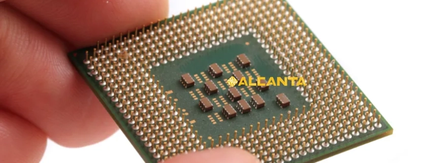
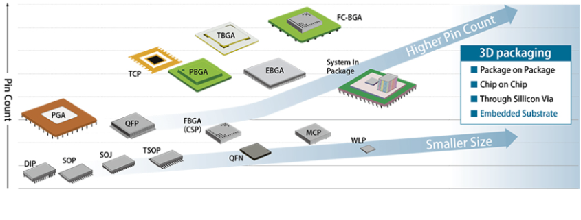
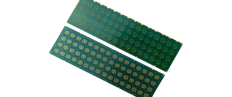
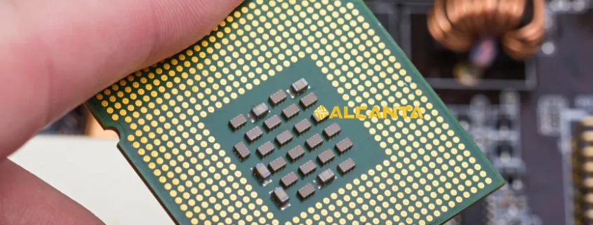
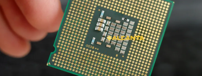
bga substrate process flow

Ball Grid Array (BGA) technology revolutionized electronic packaging by enhancing component density and reliability in electronic devices. Unlike traditional through-hole components, BGAs employ an array of solder balls beneath the component, facilitating better thermal conductivity and electrical performance. The substrate, a crucial element in BGA manufacturing, serves as the foundation for mounting integrated circuits and providing electrical connections. Its role extends beyond mere structural support; the substrate’s material composition, design, and manufacturing process significantly impact the overall performance, reliability, and manufacturability of BGA assemblies. Understanding the intricacies of substrate selection and processing is paramount in ensuring the integrity and functionality of BGA-based electronic systems.

阅读更多
bga substrate plating

In today’s advanced electronic landscape, Ball Grid Array (BGA) technology stands as a cornerstone for compact and high-performance electronic devices. BGA facilitates the dense packaging of integrated circuits (ICs) onto a single substrate, enhancing functionality while minimizing space requirements. However, amidst the intricate network of connections and components, the substrate plays a pivotal role. Serving as the foundation that hosts and interconnects various components, the substrate ensures structural integrity, electrical connectivity, and thermal management within BGA packages. Understanding the significance of the substrate is crucial for grasping the reliability and performance of BGA technology, making it a vital aspect of modern electronic manufacturing and design processes.

阅读更多
pcb substrate manufacturer

PCB substrates serve as the foundation for electronic components in printed circuit boards (PCBs), providing mechanical support and electrical insulation. Selecting the appropriate substrate is paramount, as it directly impacts the performance, reliability, and longevity of electronic devices. With a myriad of substrate materials available, such as FR-4, ceramic, and flexible materials, understanding their properties and suitability for specific applications is crucial. This guide offers an in-depth exploration of PCB substrate manufacturers, detailing their product offerings, manufacturing processes, and industry standing. By delving into the intricacies of substrate selection and the capabilities of leading manufacturers, readers can make informed decisions to optimize their PCB designs and enhance overall product quality and performance.

阅读更多
bga substrate mfg san jose

Introducing Broadpak: Pioneers of BGA Substrate Manufacturing in San Jose

Broadpak stands at the forefront of BGA substrate manufacturing in San Jose, embodying innovation and excellence in every aspect of its operations. With a rich legacy of pushing the boundaries of technology, Broadpak has established itself as a leader in the industry, delivering cutting-edge solutions to meet the evolving demands of modern electronics.

Collaboration with Altest Corporation: Elevating Standards in Substrate Production

In partnership with Altest Corporation, Broadpak continues to set new benchmarks in substrate production, combining expertise and resources to drive innovation and quality. This collaboration not only ensures the highest standards of manufacturing but also fosters a culture of continuous improvement, ultimately benefiting our customers and the industry as a whole.

阅读更多
bga substrate layout

In the realm of electronics manufacturing, the Ball Grid Array (BGA) stands as a pivotal innovation, revolutionizing how components are integrated into circuit boards. Its compact design and enhanced thermal performance have made it a cornerstone in modern electronic devices, from smartphones to aerospace equipment. However, beyond its sleek appearance lies a critical aspect often overlooked—the substrate layout. In this article, we delve into the intricate world of BGA substrate layout, exploring its profound impact on circuit performance and reliability. From understanding the materials used to optimizing ball pitch and pad layout, we unravel the complexities underlying BGA assembly. Join us on a journey to uncover the hidden intricacies of BGA substrate layout and its pivotal role in shaping the future of electronics manufacturing.

阅读更多
bga substrate layers

In today’s rapidly evolving electronics landscape, Ball Grid Array (BGA) packaging stands as a cornerstone of innovation. With its compact design and efficient heat dissipation, BGA has become ubiquitous in various electronic devices, from smartphones to high-performance computing systems. However, the true essence of BGA lies within its substrate layers, which serve as the foundation for this advanced packaging technology. These substrate layers play a pivotal role in providing structural integrity, electrical connectivity, and thermal management within the BGA package, ultimately ensuring the reliability and performance of modern electronic devices. Understanding the intricacies of BGA substrate layers is essential for comprehending the inner workings and potential applications of this groundbreaking packaging technology.

阅读更多
bga substrate cross section

In the ever-evolving landscape of modern electronics, Ball Grid Array (BGA) technology stands as a cornerstone of innovation. Its compact design, robust electrical connections, and efficient heat dissipation have revolutionized the assembly of electronic devices. However, at the heart of every BGA package lies a crucial element often overlooked: the BGA substrate cross section. This intricate layer serves as the foundation for seamless integration, facilitating electrical pathways and thermal management. Understanding the intricacies of BGA substrates is paramount in optimizing device performance, reliability, and longevity. In this blog, we delve into the depths of BGA substrate cross sections, unraveling their complexities and underscoring their indispensable role in the realm of modern electronics.

阅读更多
bga substrate crack

Ball Grid Array (BGA) technology has revolutionized electronics manufacturing with its compact design and high pin count capabilities. Widely adopted across various industries, BGAs provide efficient connectivity in devices ranging from smartphones to aerospace equipment. Central to the functionality of BGA packages is soldering, which ensures reliable electrical connections between the integrated circuits and the printed circuit board (PCB). However, despite their numerous advantages, BGA packages are susceptible to substrate cracks, presenting a significant concern in electronic assembly. Understanding the intricacies of BGA soldering and the potential risks associated with substrate cracks is crucial for ensuring the reliability and longevity of electronic products.

阅读更多
4 up flip chip bga substrate

Flip chip technology revolutionized electronic packaging by enabling smaller, faster, and more reliable devices. Unlike traditional wire bonding, flip chip bonding directly connects the chip to the substrate, enhancing electrical performance and reducing signal interference. This method finds extensive applications in microprocessors, memory chips, and high-speed communication devices. The substrate material in flip chip BGA packaging plays a crucial role in providing structural support, thermal dissipation, and electrical connectivity. Selecting the right substrate material ensures optimal performance, reliability, and manufacturability of flip chip BGA packages, making it a critical consideration in electronic design and manufacturing processes.

阅读更多
bga substrate material

Ball Grid Array (BGA) technology has revolutionized the landscape of electronic packaging, offering higher pin counts, improved electrical performance, and enhanced thermal management compared to traditional packaging methods. At the heart of BGA packages lies the substrate material, a critical component responsible for providing structural support, electrical interconnection, and thermal dissipation. The substrate material acts as a foundation for mounting integrated circuits (ICs) and forming the connection between the ICs and the printed circuit board (PCB). Therefore, understanding the significance of substrate materials in BGA packages is paramount for ensuring reliable performance and longevity of electronic devices. In this blog, we delve into the intricacies of BGA substrate materials, exploring their properties, applications, and implications for modern electronic systems.

阅读更多