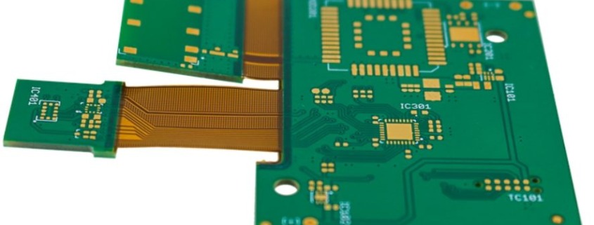
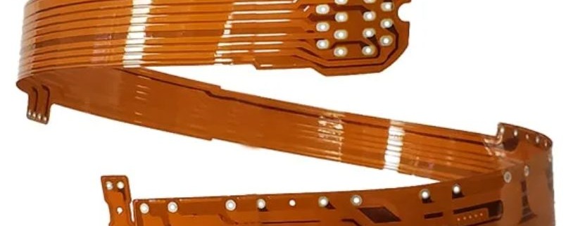
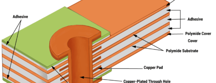
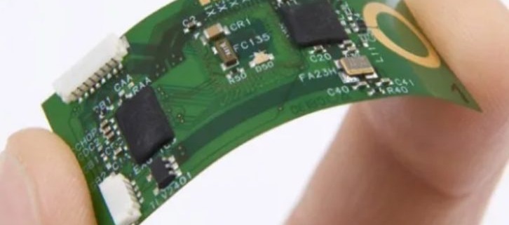
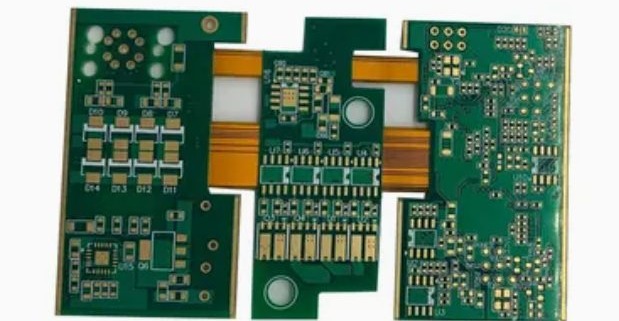
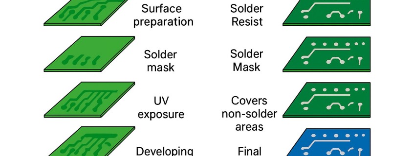
led ceramic substrate

LED ceramic substrates are specialized materials designed to support and enhance the performance of light-emitting diodes (LEDs). These substrates play a crucial role in thermal management, electrical insulation, and mechanical stability, making them essential for high-power LED applications. The unique properties of LED ceramic substrates allow for superior heat dissipation, which is vital for maintaining the longevity and efficiency of LED devices.

As the demand for advanced lighting solutions grows, the use of LED ceramic substrates in various applications—such as automotive lighting, industrial illumination, and consumer electronics—has become increasingly important. Their ability to withstand high temperatures and provide reliable performance in challenging environments gives them a significant advantage over traditional materials like FR4. In summary, LED ceramic substrates not only enhance the performance of LED technology but also contribute to the development of innovative lighting solutions in modern applications.

阅读更多
ceramic substrate manufacturing process

Ceramic substrates play a crucial role in the advancement of electronic products, offering superior thermal conductivity, mechanical stability, and resistance to harsh environments. These attributes make them ideal for applications in high-power devices, telecommunications, and automotive electronics, where reliability and performance are paramount. The ceramic substrate manufacturing process involves creating these substrates, which consist of a ceramic substrate, a connection layer, and a circuit layer. The ceramic substrate provides the foundational support, while the connection layer facilitates electrical interconnections. Finally, the circuit layer contains the printed circuitry that enables the functionality of the electronic component. Understanding the ceramic substrate manufacturing process is essential for developing high-performance electronics that meet the growing demands of modern technology. This blog post will explore the various methods used in this manufacturing process, highlighting their advantages, limitations, and applications in today’s market.

阅读更多
thin film ceramic substrates

Thin film ceramic substrates refer to specialized materials used in advanced electronics, where a thin layer of conductive material, typically copper, is deposited onto ceramic substrates like Alumina (Al2O3), Aluminum Nitride (AlN), or Silicon Nitride (SiN). These thin films range from just a few atomic layers to several microns in thickness, allowing for precise control over electrical and mechanical properties. In general, thin films are widely used due to their ability to form highly uniform and controlled coatings, essential for microelectronics. Ceramic materials play a critical role in thin film ceramic PCBs, offering excellent thermal conductivity, electrical insulation, and mechanical strength. The integration of thin film technology on ceramic substrates is crucial in harsh environments, such as aerospace, automotive, and medical applications, where performance and reliability are paramount. Thin film ceramic substrates enable the creation of high-performance electronic components that can withstand extreme conditions.

阅读更多

Rogers substrates play a crucial role in the realm of high-frequency and microwave applications, providing excellent performance and reliability. Among these materials, the Rogers 4003C substrate stands out due to its unique properties, such as a low dielectric constant and minimal loss at high frequencies. This makes it an ideal choice for various electronic applications, including RF circuit boards, telecommunications, and aerospace technologies. The ability of Rogers 4003C to maintain signal integrity while minimizing signal degradation ensures its widespread use in advanced electronic designs. As industries continue to push the boundaries of technology, the demand for high-performance materials like the Rogers 4003C substrate is expected to grow, reinforcing its significance in the electronics sector. Understanding the features and applications of this material is essential for engineers and designers looking to optimize their high-frequency designs.

阅读更多
pcb aluminium substrate

The pcb aluminium substrate is a type of metal-based circuit board that utilizes aluminium as its core material. Unlike traditional PCBs that use FR4 or other non-metallic materials, the aluminium substrate offers superior thermal conductivity and mechanical strength. The primary purpose of using a pcb aluminium substrate is to enhance heat dissipation in electronic components that generate significant heat during operation. This substrate type is particularly useful in applications where maintaining low operating temperatures is critical to prevent damage and ensure longevity.

In the electronics industry, pcb aluminium substrates are commonly found in high-power LED lighting systems, power converters, and automotive electronics, where heat management is a key consideration. By providing efficient thermal conductivity, the aluminium substrate helps protect sensitive components, allowing for higher performance and increased durability. Its ability to handle higher temperatures makes it a preferred choice for many engineers designing heat-sensitive or high-power electronic devices.

阅读更多
chip substrate manufacturers

Chip substrates are foundational materials in semiconductor manufacturing, serving as the base that supports and connects the integrated circuits (ICs) to other electronic components. They provide a platform for electrical connections and thermal dissipation, making them essential for the functionality and reliability of semiconductor devices. Without high-quality chip substrates, the performance of chips, especially in advanced electronics, would be severely compromised.

Chip substrate manufacturers play a critical role in the global supply chain by providing these essential components. Their expertise in substrate design and production directly impacts the efficiency and innovation in the semiconductor industry. As demand for smaller, faster, and more energy-efficient devices continues to grow, chip substrate manufacturers are key in enabling these advancements. Their contribution not only supports the semiconductor industry but also influences broader technology sectors, including telecommunications, consumer electronics, and automotive systems.

阅读更多
substrate-like pcb

The substrate-like PCB (SLP) is an advanced type of printed circuit board that integrates IC substrate technology to achieve higher density and miniaturization. SLP features narrower trace widths and spaces compared to traditional PCBs, allowing for more components to be placed on a smaller area. This technological advancement is crucial in meeting the increasing demand for compact, high-performance electronic devices.

The importance of substrate-like PCB technology is particularly evident in modern consumer electronics such as smartphones and wearables, where space is limited, and performance is critical. SLP enables manufacturers to create thinner, more efficient devices with enhanced functionality and lower power consumption. As the demand for smaller, more powerful electronics continues to grow, SLP plays a vital role in enabling innovations in design and performance. Its ability to support high-density integration makes it a key technology in the development of next-generation electronic products.

阅读更多
thickness of fr4 substrate

The thickness of FR4 substrate plays a critical role in printed circuit board (PCB) design, directly influencing the overall performance and reliability of electronic devices. FR4, a widely used material, is valued for its excellent insulation, flame resistance, and mechanical strength, making it the go-to choice for most PCB applications. Its thickness is not just a structural component; it also affects the electrical properties, such as signal integrity and impedance control, especially in high-frequency circuits.

Choosing the right thickness of FR4 substrate is essential, as it impacts thermal management, mechanical durability, and the ability to handle power demands. Thinner substrates are ideal for compact, lightweight designs with minimal space, while thicker substrates offer better mechanical support and heat dissipation for high-power applications. Understanding the balance between the thickness and the performance requirements of the PCB ensures the success of electronic designs in various industries.

阅读更多
alumina ceramic substrate suppliers

Alumina ceramic substrates are a key component in electronics, valued for their excellent electrical insulation, thermal conductivity, and mechanical strength. These substrates are made from alumina (Al2O3), a ceramic material known for its high dielectric constant and ability to withstand high temperatures and corrosive environments. Alumina ceramic substrates are widely used in semiconductor devices, hybrid microelectronics, and high-frequency applications, where their stability and reliability are crucial.

The global demand for alumina ceramic substrates continues to rise, driven by the growing need for high-performance materials in the electronics industry. As technology advances and miniaturization becomes more prevalent, the demand for substrates that can manage heat dissipation and ensure electrical insulation increases. Alumina ceramic substrate suppliers are at the forefront of this trend, providing the essential materials needed for devices like power modules, LED lighting, and RF components used in various high-tech industries.

阅读更多
abf substrate companies

An ABF (Ajinomoto Build-up Film) substrate is a crucial component in semiconductor packaging, providing the necessary insulation and structural support for complex electronic circuits. Developed by Ajinomoto, a Japanese company, ABF technology emerged in the late 1990s as a solution to the growing demand for miniaturized, high-performance electronic devices. ABF substrates are made from a specialized resin material that offers excellent thermal and electrical insulation properties, making them ideal for use in high-density, multi-layered PCBs (Printed Circuit Boards).

The significance of ABF substrates in electronic packaging lies in their ability to meet the rigorous demands of modern electronics, such as smartphones, servers, and AI processors. By enabling the creation of smaller, faster, and more efficient chips, ABF substrates play a pivotal role in advancing technology, driving innovation in industries ranging from consumer electronics to data centers.

阅读更多