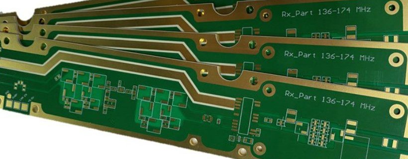
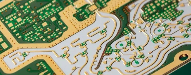
which is an advantage of the lga processor package

LGA (Land Grid Array) processor packaging has revolutionized the way processors are mounted on motherboards. Unlike traditional methods like PGA (Pin Grid Array), LGA processors feature an array of pads on the processor that make direct contact with corresponding pins on the motherboard socket. This innovation not only simplifies the manufacturing process but also enhances thermal conductivity and electrical connectivity. The history of LGA packaging traces back to the early 2000s, with Intel leading the way in its adoption. Today, LGA packaging has become the standard in modern computing systems due to its numerous advantages. In this blog, we delve into the benefits of LGA processor packaging, exploring how it improves heat dissipation, simplifies installation, and enhances overall reliability.

阅读更多
lga package

LGA (Land Grid Array) packaging is a crucial component in the electronics industry, facilitating the assembly and functioning of various electronic devices. Its significance lies in providing a reliable interface between integrated circuits and circuit boards, ensuring efficient electrical connections. LGA packaging finds extensive applications in consumer electronics, telecommunications, automotive, and industrial sectors due to its compact size, high performance, and thermal efficiency. The purpose of this introduction is to delve into the characteristics, advantages, and comparative analysis of LGA packaging against other packaging types such as BGA (Ball Grid Array) and QFN (Quad Flat No-Lead), shedding light on its unique features and suitability for diverse electronic applications.

阅读更多
interposer vs substrate

Interposers and substrates play crucial roles in semiconductor packaging, enabling advanced technologies like 2.5D CoWoS integration. Interposers serve as bridges, facilitating connections between different semiconductor components, while substrates provide structural support and electrical pathways. Understanding their significance is key to comprehending modern semiconductor packaging and testing methods.

This article provides an in-depth exploration of interposers and substrates, covering their definitions, functions, materials, applications, and a comparative analysis. By delving into these topics, readers will gain insights into the intricate world of semiconductor packaging and testing, unlocking a deeper understanding of the technologies driving innovation in the field.

阅读更多
integrated circuit substrate

Integrated Circuit (IC) substrates play a crucial role in modern electronics, serving as the foundation for the assembly and packaging of semiconductor devices. These substrates provide a platform for mounting and interconnecting integrated circuits, enabling the creation of complex electronic systems with high functionality and performance.

In this article, we will delve into the significance of IC substrates and their application areas across various industries. Additionally, we will explore the key differences between IC substrates and Printed Circuit Boards (PCBs), discuss prominent IC substrate manufacturers, examine the composition and manufacturing processes of IC substrates, and analyze future trends shaping the evolution of IC substrate technology. Through this comprehensive overview, readers will gain a deeper understanding of the critical role that IC substrates play in advancing electronic systems and driving innovation in the semiconductor industry.

阅读更多
csp chip scale package

In the realm of electronics, semiconductor packaging plays a crucial role in protecting integrated circuits (ICs) from physical damage and environmental factors, while also facilitating electrical connections. This packaging not only ensures the reliable performance of semiconductors but also enhances their compatibility with various types of electronic devices. Among the diverse packaging technologies available, Chip Scale Package (CSP) has emerged as particularly significant in modern electronics. CSP technology stands out by enabling packages that are nearly the same size as the semiconductor die they protect. This compactness is crucial for the development of smaller, more efficient, and highly integrated devices. As electronics continue to evolve towards miniaturization and higher functionality, the importance of CSP becomes increasingly pronounced, driving advancements in consumer electronics, medical devices, and automotive applications.

阅读更多
package tqfp

Semiconductor packaging serves as the bridge between integrated circuits and the outside world, ensuring their functionality, protection, and ease of integration into electronic devices. These packages come in various forms, each tailored to specific requirements and applications. Understanding package types is crucial for engineers and designers to optimize performance, reliability, and space utilization in electronic components. Among these packaging options, the TQFP (Thin Quad Flat Package) stands out for its compactness and versatility. In this blog, we delve into the significance of semiconductor packaging and highlight the importance of the TQFP package in modern electronics.

阅读更多
teflon pcb manufacturer

Teflon PCBs play a pivotal role in modern electronic applications, offering unparalleled thermal stability, electrical insulation, and signal integrity. As such, choosing the right Teflon PCB manufacturer is paramount to ensuring optimal performance and reliability in electronic devices. In this article, we delve into the significance of Teflon PCBs in today’s technology landscape, emphasizing the critical need for precision and expertise in their manufacturing process. We promise to provide a comprehensive exploration of top Teflon PCB manufacturers, highlighting their capabilities, quality standards, and contributions to the industry. Whether you’re seeking high-frequency applications or demanding environments, selecting the right Teflon PCB manufacturer is key to unlocking the full potential of your electronic designs.

阅读更多
substrate pcb

PCB Substrate serves as the foundation of a printed circuit board (PCB), providing mechanical support and electrical connectivity for electronic components. Its significance lies in ensuring the structural integrity of the PCB while facilitating the transmission of signals between components. Functionally, Substrate PCB acts as a dielectric material between copper traces, preventing short circuits and facilitating the flow of electrical signals across the board. Moreover, it influences the PCB’s thermal and electrical performance, affecting factors like signal integrity and reliability. Understanding the role of Substrate PCB is crucial in optimizing circuit board design for various applications, ensuring robust performance and longevity of electronic devices.

阅读更多
chip on board process

Chip on Board (COB) technology revolutionizes traditional electronic packaging by directly mounting semiconductor chips onto a substrate. This method eliminates the need for individual packaging, leading to a compact, efficient design. COB has evolved from its inception in the late 20th century to become a cornerstone of modern electronics, offering significant advancements in miniaturization, performance, and reliability. Its application extends beyond electronics, particularly in LED lighting where COB configurations deliver unparalleled brightness and energy efficiency. Moreover, COB technology finds utility in various fields like automotive, medical devices, and consumer electronics, emphasizing its versatility and indispensability in contemporary engineering.

阅读更多
chipsmall limited

Introducing emerging technological products is pivotal for steering technological advancements. In today’s digital landscape, the emergence of 3D IC Package Substrate stands as a testament to innovation in the electronics sector. This article embarks on an exploration of this groundbreaking technology, unraveling its intricacies and unveiling its myriad potential applications. From its inception to its current advancements, we’ll delve deep into the realm of 3D IC Package Substrate, shedding light on the transformative impact it promises to have on various industries. Join us on this journey as we uncover the fascinating world of 3D IC Package Substrate and its role in shaping the future of technology.

阅读更多