
Exploring Advanced Flip Chip Packaging Technology
In recent decades, flip chip packaging technology has emerged as a pivotal advancement in the realm of semiconductor packaging. Initially conceived in the late 1960s, its development gained momentum with the miniaturization and increasing complexity of electronic devices. Unlike conventional packaging methods, flip chip technology allows for direct electrical connections between the chip and substrate, enhancing performance, reliability, and thermal management.
In the electronics industry, where demands for smaller form factors, higher performance, and lower costs persist, flip chip packaging has become indispensable. From smartphones and laptops to automotive electronics and medical devices, its applications span across various sectors, driving innovation and pushing the boundaries of what’s achievable in electronic design. Understanding the evolution and significance of flip chip packaging technology unveils its transformative impact on modern electronics.
What is Flip Chip Packaging Technology?
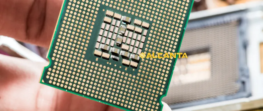
Flip chip packaging technology revolutionizes the traditional approach to semiconductor packaging by flipping the chip upside down and mounting it directly onto the substrate or circuit board. This method involves connecting the active side of the chip to the substrate using conductive bumps, typically made of solder or copper pillars.
Basic Principles:
The fundamental principle of flip chip packaging involves the direct electrical connection between the chip and the substrate, eliminating the need for wire bonds. This allows for shorter interconnection lengths, reducing parasitic effects and improving signal integrity.
Comparison with Traditional Packaging Techniques:
In contrast to traditional packaging techniques like wire bonding, where wires are connected from the chip’s periphery to the substrate, flip chip packaging offers several advantages. It enables higher interconnection density, better thermal management, and improved electrical performance due to shorter signal paths. Additionally, flip chip packaging facilitates the integration of multiple chips into a single package, known as System in Package (SiP), enhancing functionality while reducing footprint.
Advantages and Characteristics:
Higher Interconnection Density: Flip chip packaging allows for a higher number of interconnects per unit area compared to wire bonding, enabling the integration of more complex circuits in smaller packages.
Improved Thermal Performance: Direct attachment of the chip to the substrate enhances heat dissipation, reducing thermal resistance and improving overall device reliability.
Enhanced Electrical Performance: Shorter interconnection lengths in flip chip packaging result in lower parasitic effects, leading to improved signal integrity and higher operating frequencies.
SiP Integration: Flip chip packaging enables the integration of multiple chips within the same package, facilitating the development of highly integrated and multifunctional devices.
Understanding these principles and advantages elucidates the transformative potential of flip chip packaging technology in advancing the capabilities of electronic devices.
C4 Bump Technology
Definition and Purpose of C4 Bump Technology:
C4 (Controlled Collapse Chip Connection) Bump technology, also known as solder bump technology, is a crucial aspect of flip chip packaging. It involves the deposition of small solder bumps onto the active surface of the semiconductor chip, which serve as the electrical connections between the chip and the substrate or circuit board. The purpose of C4 Bump technology is to provide reliable electrical connections while accommodating for the differences in thermal expansion between the chip and the substrate.
Working Principles of C4 Bump Technology:
The process of creating C4 bumps typically involves several steps, including solder deposition, bump formation, and reflow soldering. First, solder material is deposited onto the chip’s bonding pads using techniques like electroplating or solder paste printing. Then, the deposited solder is shaped into bumps through processes such as stencil printing or solder ball placement. During reflow soldering, the entire assembly undergoes controlled heating, causing the solder bumps to melt and form intermetallic bonds with both the chip and the substrate.
The key principle behind C4 Bump technology lies in the controlled collapse of the solder bumps during reflow, ensuring proper alignment and connection between the chip and the substrate. The controlled collapse prevents excessive solder spreading and bridging between adjacent bumps, maintaining the integrity of the electrical connections.
Application Cases of C4 Bump Technology in Advanced Flip Chip Packaging:
C4 Bump technology finds widespread applications in various advanced flip chip packaging scenarios. For instance:
1. High-performance microprocessors: C4 Bump technology enables the assembly of high-density interconnections, allowing for the integration of complex microprocessor units with superior electrical performance and thermal management.
2. Graphics processing units (GPUs): In graphics cards and other high-speed computing applications, C4 Bump technology facilitates the connection of GPU chips to the substrate, ensuring reliable data transmission and efficient heat dissipation.
3. Memory modules: Advanced memory modules, such as DRAM and NAND flash, utilize C4 Bump technology to achieve high-speed data transfer rates and compact form factors, meeting the demands of modern computing and mobile devices.
These examples underscore the critical role of C4 Bump technology in enabling the development of advanced flip chip packaging solutions for a wide range of electronic applications.
SiP (System in Package) Modules
Concept and Features of SiP Modules:
System in Package (SiP) modules represent an advanced packaging approach where multiple chips, along with other passive components, are integrated into a single package. Unlike traditional packaging methods where each chip is packaged individually, SiP modules enable the creation of highly integrated systems by stacking, embedding, or arranging chips within a compact package. This integration offers several advantages, including reduced footprint, improved signal integrity, and enhanced performance.
Key features of SiP modules include:
High Integration Density: SiP modules allow for the integration of multiple chips, such as microprocessors, memory, and sensors, into a single package, reducing the overall size of the electronic system.
Interconnect Flexibility: SiP modules provide flexibility in interconnecting different components using various methods, including wire bonding, flip chip bonding, and through-silicon vias (TSVs), enabling customized designs for specific applications.
Mixed-Signal Integration: SiP modules facilitate the integration of both digital and analog components within the same package, enabling the development of complex systems with diverse functionalities.
Structure and Components of SiP Modules:
The structure of SiP modules typically comprises multiple layers, each housing different components and interconnects. The key components include:
Chips: Various semiconductor chips, such as microprocessors, memory, sensors, and RF modules, are integrated into the SiP module.
Passive Components: These include resistors, capacitors, and inductors, which are essential for signal conditioning, filtering, and power management.
Interconnects: Interconnections between components are established using techniques such as wire bonding, flip chip bonding, or through-silicon vias (TSVs).
Substrate: The substrate provides mechanical support and electrical connections between the components and external interfaces.
Application Scenarios of SiP Modules in Advanced Flip Chip Packaging:
SiP modules find extensive application in various advanced flip chip packaging scenarios, including:
1. Mobile Devices: In smartphones and tablets, SiP modules integrate multiple functionalities, such as application processors, memory, RF transceivers, and power management units, into a compact package, enabling high-performance and energy-efficient devices.
2. Wearable Electronics: SiP modules are utilized in wearable devices, such as smartwatches and fitness trackers, to integrate sensors, microcontrollers, and wireless communication modules, providing advanced functionalities in a small form factor.
3. Internet of Things (IoT) Devices: In IoT applications, SiP modules enable the integration of sensing, processing, and communication capabilities into a single package, facilitating the deployment of smart and connected devices in various industries, including healthcare, agriculture, and industrial automation.
These examples highlight the versatility and versatility of SiP modules in enabling the development of advanced flip chip packaging solutions for diverse electronic applications.
Applications of Advanced Flip Chip Packaging Technology
Case Studies of Advanced Flip Chip Packaging Technology in Electronic Products:
1. Smartphones: Advanced flip chip packaging technology has revolutionized the design and performance of smartphones. For example, in flagship smartphones, the application processor, graphics processor, memory modules, and other essential components are integrated using flip chip packaging, allowing for high-speed data processing, improved power efficiency, and compact form factors.
2. Automotive Electronics: In the automotive industry, advanced flip chip packaging plays a vital role in enhancing the performance and reliability of electronic control units (ECUs) and sensors. By utilizing flip chip technology, automotive manufacturers can achieve robust connections, withstand harsh environmental conditions, and reduce the size and weight of electronic components, contributing to improved vehicle safety and efficiency.
3. Data Centers: Advanced flip chip packaging technology is widely adopted in data center infrastructure, where high-performance computing is crucial. By employing flip chip packaging for processors, memory modules, and networking components, data centers can achieve higher processing speeds, reduced latency, and improved energy efficiency, enabling seamless operation of cloud computing services and big data analytics.
Enhancement of Product Performance and Functionality through Advanced Flip Chip Packaging Technology:
1. Improved Thermal Management: Advanced flip chip packaging technology enables efficient heat dissipation, reducing thermal resistance and improving the overall thermal performance of electronic devices. This leads to increased reliability and longevity of components, particularly in high-power applications such as servers, gaming consoles, and automotive electronics.
2. Enhanced Signal Integrity: By minimizing the length of interconnects and reducing parasitic effects, advanced flip chip packaging technology enhances signal integrity, enabling high-speed data transmission and reducing electromagnetic interference (EMI). This is critical for applications requiring high bandwidth and reliability, such as telecommunications equipment and networking devices.
3. Compact Form Factors: Advanced flip chip packaging allows for higher integration density and smaller form factors, enabling the development of more compact and lightweight electronic products. This is especially beneficial for portable devices such as smartphones, tablets, and wearable electronics, where size and weight constraints are significant considerations.
4. Increased Functionality: By integrating multiple chips and components within a single package, advanced flip chip packaging technology enables the development of highly integrated systems with enhanced functionality. This enables the creation of multifunctional devices capable of performing a wide range of tasks, such as image processing, artificial intelligence, and sensor fusion, in diverse application domains.
Overall, advanced flip chip packaging technology not only improves the performance and functionality of electronic products but also enables manufacturers to meet the evolving demands of consumers for smaller, faster, and more capable devices.
Future Prospects of Advanced Flip Chip Packaging Technology
Trends in the Development of Advanced Flip Chip Packaging Technology:
1. Increased Integration Density: One of the prominent trends in advanced flip chip packaging technology is the continual pursuit of higher integration density. This involves packing more components, including chips, passive components, and interconnects, into smaller packages, enabling the development of ultra-compact and highly integrated electronic systems.
2. Advanced Materials and Processes: The adoption of novel materials and manufacturing processes is another key trend in the development of advanced flip chip packaging technology. This includes the exploration of new solder alloys, conductive adhesives, and dielectric materials, as well as the advancement of additive manufacturing techniques such as 3D printing and laser direct structuring.
3. Heterogeneous Integration: Heterogeneous integration, which involves combining chips with different technologies, functionalities, and materials within the same package, is gaining traction in advanced flip chip packaging. This approach enables the integration of diverse components, such as silicon chips, III-V compound semiconductors, and MEMS devices, to realize multifunctional and high-performance electronic systems.
Prospects for the Application of Advanced Flip Chip Packaging Technology in Next-Generation Electronic Products:
1. 5G and Beyond: With the rollout of 5G networks and the emergence of new wireless communication standards, there is a growing demand for advanced flip chip packaging technology in next-generation mobile devices, base stations, and IoT devices. Flip chip packaging enables the integration of high-frequency RF components, such as power amplifiers, filters, and antennas, to support the increased data rates and network capacity of 5G systems.
2. Artificial Intelligence (AI) and Machine Learning: Advanced flip chip packaging technology is poised to play a crucial role in the development of AI and machine learning systems. By integrating specialized AI accelerators, such as neuromorphic chips and tensor processing units (TPUs), into compact and energy-efficient packages, flip chip packaging enables the deployment of AI-enabled devices for edge computing, autonomous vehicles, and smart robotics.
3. Healthcare and Biomedical Devices: In the healthcare sector, advanced flip chip packaging technology holds promise for the development of miniaturized and wearable biomedical devices for monitoring, diagnosis, and treatment. By integrating sensors, microfluidic channels, and bioelectronic components within compact and biocompatible packages, flip chip packaging enables the realization of personalized and point-of-care medical devices for improved patient outcomes.
Potential Innovations and Improvement Directions:
1. Advanced Interconnect Technologies: Continued innovation in interconnect technologies, such as copper pillar bumping, microbumps, and through-silicon vias (TSVs), will enable higher bandwidth, lower latency, and improved reliability in advanced flip chip packaging.
2. Embedded Cooling Solutions: The development of embedded cooling solutions, such as microfluidic channels and integrated heat sinks, will address the thermal challenges associated with high-power flip chip packages, enabling higher performance and longer device lifetimes.
3. Design for Manufacturability (DfM): Enhancements in design for manufacturability (DfM) tools and methodologies will streamline the development and fabrication of advanced flip chip packages, reducing time-to-market and manufacturing costs while ensuring high yields and product reliability.
Overall, the future of advanced flip chip packaging technology is bright, with ongoing research and development efforts poised to drive further innovation and enable the realization of next-generation electronic products with unprecedented performance, functionality, and miniaturization.
FAQs about Advanced Flip Chip Packaging
Flip chip packaging is a semiconductor packaging technique where the active side of the chip is flipped and mounted directly onto the substrate or circuit board. This differs from traditional packaging methods such as wire bonding, where wires are connected from the chip’s periphery to the substrate. Flip chip packaging offers advantages like higher interconnection density, improved thermal management, and enhanced electrical performance due to shorter signal paths.
C4 bumps, or Controlled Collapse Chip Connection bumps, are small solder bumps deposited onto the active surface of the semiconductor chip in flip chip packaging. They serve as the electrical connections between the chip and the substrate. C4 bumps are crucial because they enable reliable electrical connections while accommodating for the differences in thermal expansion between the chip and the substrate.
SiP modules integrate multiple chips, along with other passive components, into a single package. Flip chip packaging is often used in SiP modules to achieve high-density interconnections between the chips and the substrate. SiP modules enable the development of highly integrated systems with reduced footprint and improved functionality, making them ideal for applications where space constraints are critical.
Advanced flip chip packaging technology improves product performance and functionality in several ways. It enables improved thermal management, enhanced signal integrity, compact form factors, and increased functionality through the integration of multiple chips and components within a single package. These advancements lead to higher performance, greater reliability, and more innovative electronic products.


发表评论
Want to join the discussion?Feel free to contribute!