
Elevating Performance: Advanced Cavity PCB Manufacturing
In the rapidly evolving landscape of modern electronics, Advanced Cavity PCBs (Printed Circuit Boards) stand as a testament to innovation and precision engineering. These specialized boards integrate intricately designed cavities within their structure, revolutionizing thermal management, electromagnetic compatibility, and overall performance. As industries across the globe increasingly rely on intricate electronic systems, the demand for sophisticated PCBs continues to soar. From aerospace and automotive to medical devices and consumer electronics, the need for highly reliable, compact, and efficient PCB solutions has become paramount. Advanced Cavity PCBs emerge as a cornerstone technology meeting these evolving demands, offering unparalleled versatility and functionality in an ever-expanding array of applications.
Understanding Advanced PCB Manufacturing
Defining PCBs and Their Primary Function
Printed Circuit Boards (PCBs) serve as the backbone of electronic devices, providing a platform for the interconnection of electronic components. These boards are composed of non-conductive substrate material, typically fiberglass, with copper traces etched onto their surface to create conductive pathways. PCBs facilitate the efficient flow of electrical signals between components, ensuring proper functionality and performance in electronic devices of all kinds.
B. Evolution of PCB Manufacturing Techniques
The journey of PCB manufacturing has seen remarkable advancements over the years. Initially, PCBs were produced using labor-intensive methods like point-to-point wiring, which were inefficient and prone to errors. With the advent of automated etching and drilling processes in the mid-20th century, mass production became more feasible, enabling the widespread adoption of PCBs in various industries.
As technology progressed, so did PCB manufacturing techniques. Innovations such as surface mount technology (SMT), through-hole plating, and multilayer PCBs allowed for denser component placement and improved signal integrity. These developments laid the foundation for the emergence of advanced cavity PCBs, where precision and complexity play pivotal roles in meeting the demands of modern electronics.
Importance of Precision and Complexity in Modern PCB Designs
In today’s electronic landscape, precision and complexity are paramount in PCB design and manufacturing. Miniaturization trends demand increasingly compact PCB layouts, necessitating intricate routing and component placement to maximize space utilization without compromising functionality. Moreover, as electronic devices become more powerful and versatile, PCBs must accommodate higher frequencies, tighter tolerances, and advanced features like impedance control and signal integrity management.
Advanced cavity PCBs embody the pinnacle of precision and complexity in PCB design. By integrating specialized cavities within the board structure, these PCBs offer enhanced thermal management, reduced electromagnetic interference, and improved mechanical stability. Achieving such feats requires state-of-the-art manufacturing processes, meticulous attention to detail, and a deep understanding of electrical engineering principles.
In essence, the evolution of PCB manufacturing has been driven by the relentless pursuit of precision and complexity, culminating in the development of advanced cavity PCBs that push the boundaries of what’s possible in modern electronics.
Exploring Cavity PCBs
Understanding PCB Cavities
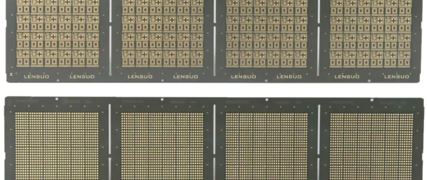
In the realm of PCB design, a “cavity” refers to a recessed area within the board’s substrate, typically created by milling or drilling processes. These cavities can vary in size, shape, and depth, depending on the specific requirements of the application. In advanced designs, cavities are strategically incorporated to accommodate various components, such as microprocessors, sensors, or connectors, while optimizing space utilization and enhancing performance.
Benefits of Incorporating Cavities in PCBs
1. Improved Thermal Management: Cavities in PCBs facilitate better heat dissipation by creating additional surface area for heat transfer. This is particularly crucial in high-power applications where efficient thermal management is essential to prevent component overheating and ensure reliability.
2. Reduced Electromagnetic Interference (EMI): By isolating sensitive components within cavities, PCBs can effectively shield them from external electromagnetic interference sources. This helps minimize signal degradation and ensures the integrity of critical electronic circuits, especially in environments with high EMI levels.
3. Enhanced Mechanical Stability: Cavities add structural reinforcement to PCBs, enhancing their mechanical stability and resistance to physical stressors such as vibration, shock, and bending. This is particularly advantageous in rugged environments or applications where reliability is paramount, such as automotive electronics or aerospace systems.
4. Space Optimization: Cavities allow for compact and efficient PCB layouts by accommodating bulky components or integrating additional functionality within the board’s footprint. This enables designers to create more streamlined and integrated electronic systems without compromising performance or reliability.
In summary, the strategic integration of cavities in PCBs offers a myriad of benefits that contribute to the overall performance, reliability, and versatility of advanced electronic devices. From improved thermal management to enhanced EMI shielding and mechanical stability, cavity PCBs represent a cutting-edge solution for meeting the demanding requirements of modern electronics applications.
Differentiating PCBs and HDI PCBs
Understanding HDI PCBs
High-Density Interconnect (HDI) PCBs represent a significant advancement in PCB technology, specifically designed to accommodate the increasing demand for miniaturization and high-performance electronics. HDI PCBs utilize advanced manufacturing techniques and materials to achieve higher component density and more intricate routing capabilities compared to traditional PCBs.
Key Features of HDI PCBs include:
1. Microvias: HDI PCBs leverage microvias, which are tiny drilled holes with diameters typically less than 150 microns, to facilitate interconnections between layers. These microvias enable denser routing and allow for more compact designs compared to through-hole vias used in conventional PCBs.
2. Layer Count: HDI PCBs often feature multiple layers with densely packed circuitry, allowing for greater design flexibility and functionality in a smaller footprint. This increased layer count enables designers to integrate complex electronic systems with minimal space requirements.
3. Fine Line and Spacing: HDI PCBs can achieve finer line widths and spacing between traces, allowing for tighter routing and higher interconnect densities. This capability enables the design of high-speed digital circuits with improved signal integrity and reduced electromagnetic interference.
Distinctions between Conventional PCBs and HDI PCBs
1. Technology: Conventional PCBs typically utilize through-hole technology and larger vias for interconnection between layers, whereas HDI PCBs leverage advanced manufacturing techniques such as laser drilling and sequential lamination to implement microvias and achieve higher component density.
2. Complexity: HDI PCBs offer greater complexity in terms of layer count, routing density, and miniaturization compared to conventional PCBs. They can accommodate a larger number of components and interconnections in a smaller space, making them ideal for applications requiring high functionality in compact form factors.
3. Applications: While conventional PCBs are suitable for a wide range of applications, including consumer electronics, automotive, and industrial controls, HDI PCBs are particularly well-suited for high-performance devices such as smartphones, tablets, wearables, medical devices, and aerospace systems. Their ability to meet stringent size, weight, and performance requirements makes them indispensable in modern electronics design.
In essence, HDI PCBs represent a paradigm shift in PCB technology, offering unparalleled levels of miniaturization, performance, and functionality compared to conventional PCBs. As the demand for smaller, more powerful electronic devices continues to grow, HDI PCBs will play an increasingly vital role in enabling the next generation of advanced electronics.
Unveiling CCA PCBs
Defining CCA PCBs and Their Role in Advanced Electronics
Component Carrier Assembly (CCA) PCBs represent a sophisticated approach to electronic assembly, where individual components are mounted directly onto the PCB substrate rather than being soldered onto the surface. In CCA PCBs, the components are embedded within the board structure, providing several advantages in terms of miniaturization, performance, and reliability.
Unique Features and Advantages of CCA PCBs
1. Miniaturization: CCA PCBs enable significant reductions in overall size and weight compared to traditional PCB assemblies. By integrating components directly into the board substrate, CCA PCBs eliminate the need for bulky external components and connectors, resulting in more compact and streamlined electronic systems.
2. Enhanced Performance: The close proximity of components to the PCB substrate in CCA designs reduces parasitic capacitance and inductance, leading to improved signal integrity and faster signal propagation. This results in higher performance and reliability, making CCA PCBs ideal for applications requiring high-speed data transmission or precision analog circuitry.
3. Improved Thermal Management: CCA PCBs offer superior thermal management capabilities compared to traditional PCB assemblies. By embedding components within the board substrate, heat dissipation is more efficient, leading to lower operating temperatures and increased reliability, particularly in high-power applications.
4. Increased Reliability: The integration of components directly into the PCB substrate enhances the overall robustness and durability of CCA PCBs. With fewer external connections and points of failure, CCA designs exhibit greater resistance to mechanical stress, vibration, and environmental factors, resulting in improved long-term reliability and product lifespan.
5. Design Flexibility: CCA PCBs offer designers greater flexibility in terms of layout and component placement. By embedding components within the board substrate, designers can achieve more creative and innovative designs, optimizing space utilization and enhancing overall system performance.
In summary, CCA PCBs represent a groundbreaking approach to electronic assembly, offering unparalleled levels of miniaturization, performance, and reliability. With their unique features and advantages, CCA PCBs are poised to revolutionize the way advanced electronics are designed and manufactured, enabling the development of smaller, faster, and more reliable electronic systems across a wide range of applications.
Exploring Complexity in PCBs
Factors Contributing to Complexity in PCB Designs
1. Component Density: As electronic devices continue to shrink in size, PCB designers are challenged with packing increasingly more components into smaller spaces. This requires intricate routing and placement techniques to ensure optimal performance while avoiding signal interference and thermal issues.
2. High-Speed Design Requirements: With the proliferation of high-speed data transmission in modern electronics, PCBs must adhere to stringent signal integrity requirements. Designing for high-speed signals involves careful consideration of impedance control, signal propagation delay, and crosstalk mitigation, adding layers of complexity to PCB layouts.
3. Multilayer Architecture: Complex electronic systems often require multilayer PCBs to accommodate the large number of components and interconnections. Managing the interactions between multiple signal layers, power planes, and ground planes introduces challenges in ensuring signal integrity and power distribution throughout the board.
4. Advanced Manufacturing Techniques: The adoption of advanced manufacturing processes such as HDI (High-Density Interconnect), sequential lamination, and microvia drilling enables greater miniaturization and component density in PCB designs. However, these techniques also require precise control and coordination to achieve desired results, adding complexity to the manufacturing process.
Examples of the Most Complex PCBs
1. Smartphones and Mobile Devices: PCBs found in smartphones and other mobile devices are among the most complex due to their compact form factor and high-performance requirements. These PCBs incorporate a multitude of components, including processors, memory modules, sensors, and communication interfaces, all within a limited space.
2. High-Performance Computing (HPC) Systems: PCBs used in HPC systems, such as supercomputers and data centers, are designed to handle massive amounts of data and computational tasks. These PCBs feature dense component layouts, high-speed interconnects, and advanced thermal management solutions to support the demanding computational workloads.
3. Medical Devices: PCBs used in medical devices, such as MRI machines, CT scanners, and implantable devices, must meet strict reliability and safety standards while also delivering high performance. These PCBs often incorporate complex analog and digital circuitry, as well as specialized sensors and interfaces, to ensure accurate and reliable operation in medical settings.
4. Aerospace and Defense Systems: PCBs used in aerospace and defense applications demand ruggedness, reliability, and high performance in extreme environments. These PCBs must withstand shock, vibration, temperature extremes, and radiation, while also incorporating advanced features such as embedded sensors, encryption, and secure communication protocols.
In conclusion, the complexity of PCB designs is driven by a combination of factors including component density, high-speed design requirements, multilayer architecture, and advanced manufacturing techniques. Examples of the most complex PCBs span across various industries, from smartphones and HPC systems to medical devices and aerospace applications, highlighting the critical role of PCB technology in enabling cutting-edge advancements in modern electronics.
Leading Advanced Cavity PCB Manufacturers
Overview of Reputable PCB Manufacturers
In the realm of advanced cavity PCB manufacturing, several companies stand out for their expertise, innovation, and commitment to quality. These manufacturers leverage cutting-edge technology and extensive experience to produce high-performance PCBs tailored to the unique requirements of modern electronics applications.
Highlight of Companies in the USA
1. Advanced Circuits: Based in Colorado, Advanced Circuits is one of the leading PCB manufacturers in the USA, known for its advanced capabilities in producing high-quality cavity PCBs. The company offers a wide range of services, including quick-turn prototypes, multilayer PCBs, and advanced HDI designs. Advanced Circuits is renowned for its fast turnaround times, exceptional customer service, and commitment to innovation.
2. Rogers Corporation: Rogers Corporation, headquartered in Arizona, specializes in advanced materials for PCB manufacturing, including high-frequency laminates and thermal management solutions. With a focus on innovation and collaboration, Rogers Corporation works closely with customers to develop customized solutions for demanding applications in aerospace, automotive, and telecommunications.
Highlight of Companies in Europe
1. Eurocircuits: Based in Belgium, Eurocircuits is a leading PCB manufacturer in Europe, offering a wide range of advanced cavity PCB solutions. The company’s portfolio includes multilayer PCBs, flexible PCBs, and rigid-flex PCBs, all manufactured using state-of-the-art equipment and processes. Eurocircuits is known for its fast turnaround times, competitive pricing, and commitment to environmental sustainability.
2. Isola Group: Isola Group, headquartered in Switzerland, is a global leader in high-performance PCB materials and solutions. The company specializes in advanced laminates for cavity PCBs, offering exceptional thermal conductivity, electrical performance, and reliability. With a strong focus on research and development, Isola Group continually pushes the boundaries of PCB technology to meet the evolving needs of the electronics industry.
In summary, the USA and Europe are home to several reputable PCB manufacturers specializing in advanced cavity PCBs. Companies like Advanced Circuits, Rogers Corporation, Eurocircuits, and Isola Group exemplify excellence in PCB manufacturing, showcasing their expertise, capabilities, and technological advancements to drive innovation and advancement in the electronics industry.
FAQs about Advanced Cavity PCB Manufacturer
A cavity in a PCB refers to a recessed area within the board’s substrate, typically created by milling or drilling processes. These cavities can vary in size, shape, and depth and are strategically incorporated to accommodate various components while optimizing space utilization and enhancing performance.
The main difference between a PCB and an HDI PCB lies in their construction and capabilities. While a conventional PCB (Printed Circuit Board) typically uses through-hole technology and larger vias for interconnection between layers, an HDI PCB (High-Density Interconnect PCB) leverages advanced manufacturing techniques such as microvias, sequential lamination, and fine line and spacing to achieve higher component density and more intricate routing capabilities.
CCA PCB stands for Component Carrier Assembly PCB. It represents a sophisticated approach to electronic assembly where individual components are mounted directly onto the PCB substrate rather than being soldered onto the surface. In CCA PCBs, the components are embedded within the board structure, offering advantages in terms of miniaturization, performance, and reliability.
Identifying the “most complex” PCB is subjective and can vary depending on factors such as application, industry, and specific requirements. PCBs used in smartphones, high-performance computing systems, medical devices, and aerospace applications are typically considered complex due to their dense component layouts, high-speed design requirements, and stringent reliability standards.

