
Key Considerations in High Frequency PCB Manufacturing for 5G
Printed Circuit Boards (PCBs) are fundamental to modern electronics, serving as the backbone for connecting and supporting electronic components. As technology advances, the demand for high-performance circuits has grown, especially in high-frequency applications such as 5G networks, radar systems, satellites, and other RF technologies. High-frequency PCB manufacturing plays a critical role in meeting the stringent requirements of these applications. These specialized PCBs are designed to minimize signal loss, interference, and degradation at high speeds, ensuring reliable and efficient performance. With the rise of high-speed communications and advanced radar technologies, high-frequency PCBs are essential for supporting innovations in telecommunications, aerospace, and automotive industries. The need for precise materials, optimized design, and advanced manufacturing techniques has made specialized PCB manufacturing for high-frequency circuits a key focus in modern electronics development.
What is a High Frequency PCB? Understanding the Foundation of High Frequency PCB Manufacturing
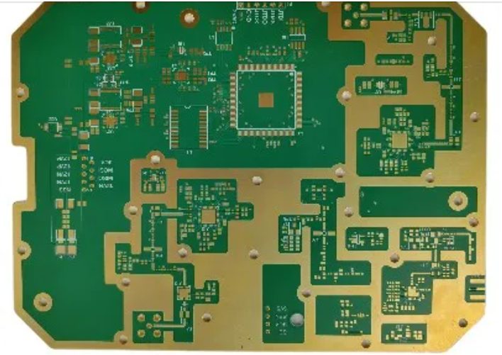
In the context of modern electronics, a high frequency PCB refers to a printed circuit board that is specifically designed to carry signals at frequencies typically above 1 GHz. These PCBs are essential in applications like satellite communications, RF systems, automotive radar, and 5G infrastructure, where signal accuracy and transmission speed are paramount.
Unlike standard PCBs, which use common FR4 materials and are optimized for lower-speed digital signals, high frequency PCBs require specialized materials and more precise fabrication methods. This is where high frequency pcb manufacturing plays a crucial role—ensuring low signal loss, stable performance, and minimal electromagnetic interference.
Materials such as PTFE (Teflon), Rogers laminates, High Temp FR4, and ceramic-filled substrates are commonly used due to their low dielectric constant (Dk) and dissipation factor (Df). A low and stable Dk ensures consistent impedance, while a low Df minimizes signal attenuation, both essential for reliable high-frequency operation. Thus, high frequency pcb manufacturing is not just about building a board—it’s about enabling precision-driven performance at the speed of innovation.
High-Frequency PCB Design Guide: Core to High Frequency PCB Manufacturing
Effective PCB design is at the heart of successful high frequency pcb manufacturing. The performance of high-speed and RF circuits relies not only on the materials chosen but also on the precision of the layout and stackup. Below is a detailed design guide to address the most critical aspects:
Material Selection
In high frequency pcb manufacturing, selecting materials with consistent dielectric properties is essential. Variations in the dielectric constant (Dk) can cause impedance mismatches and degrade signal integrity. Materials like PTFE (Teflon) offer excellent electrical properties but can be more difficult to process. On the other hand, High Temp FR4 provides better mechanical stability and cost-efficiency, though with slightly higher signal loss. The choice depends on application frequency, cost constraints, and fabrication capabilities.
Signal Integrity (SI)
Maintaining signal integrity is critical in high frequency pcb manufacturing. This involves controlled impedance routing, ensuring that trace width and spacing align with target impedance values (typically 50Ω or 100Ω differential). Design techniques must also mitigate reflection, crosstalk, and electromagnetic interference (EMI). Incorporating differential pair routing with tightly coupled traces helps suppress noise and maintain timing integrity in high-speed signals.
Layer Stackup & HDI Design
A well-planned layer stackup provides signal isolation and reduces EMI. In high frequency pcb manufacturing, designers often use multi-layer structures with solid ground planes adjacent to signal layers. Blind and buried vias, along with microvias, are common in HDI PCB designs, allowing for higher routing density and better electrical performance. These features help minimize via stubs and maintain clean signal transitions between layers.
High-Speed Design Techniques
To ensure signal quality in high-speed systems, ground plane continuity must be preserved beneath critical signal paths. Proper return path management ensures that high-frequency currents flow predictably, minimizing loop area and EMI. In PCB manufacturing, via design is carefully optimized to reduce parasitic inductance and reflection—techniques include back-drilling, via-in-pad, and stub elimination.
Every design decision directly impacts the success of the manufacturing process, making collaboration between designers and fabricators essential from the earliest stages.
Manufacturing Process for High Frequency PCBs: Mastering High Frequency PCB Manufacturing Techniques
Achieving high-performance results in high frequency pcb manufacturing requires more than just good design—it demands advanced processing technologies, high-precision control, and expert material handling. Below, we explore the key aspects of the manufacturing process that ensure the integrity and reliability of high-frequency circuits.
Material Handling Challenges
One of the most critical challenges in high frequency pcb manufacturing is working with non-standard materials such as PTFE and ceramic-filled laminates. These substrates offer superior electrical properties but are mechanically soft and prone to deformation during drilling and routing. Specialized machining tools and slower processing speeds are often required. Additionally, achieving strong adhesion between copper and these low-surface-energy materials demands surface treatments like plasma activation or chemical etching. Without proper handling, long-term stability and layer bonding can become reliability risks.
Precision Etching & Impedance Control
In high-speed designs, trace width tolerances must be tightly controlled to maintain consistent impedance. In high frequency pcb manufacturing, even slight deviations can cause reflection and signal degradation. To achieve the required precision, manufacturers use laser direct imaging (LDI), plasma etching, and advanced photolithography. Post-etch, in-process impedance testing—using Time Domain Reflectometry (TDR) or Vector Network Analysis (VNA)—ensures every board meets the target impedance specifications before moving to assembly.
Integration with Rigid-Flex and LED PCBs
Combining rigid-flex PCB technology with high-frequency circuitry offers space savings and design flexibility, especially in aerospace, military, and medical applications. However, integrating flexible layers with high-speed signals in high frequency pcb manufacturing introduces challenges like material mismatch and controlled bend radius constraints. For LED PCBs, which often handle both high power and high frequency, thermal management is key. Proper heat dissipation techniques—such as metal-core substrates or thermal vias—are essential to prevent performance degradation due to overheating.
Fast Turn PCB Manufacturing
In today’s fast-paced development cycles, fast turn PCB production is often required. While speed is critical, it must not come at the cost of quality—especially in high-frequency applications, where accuracy in layer registration, via quality, and impedance control cannot be compromised. Quick-turn services should still provide full DFM checks, material traceability, and electrical testing to ensure the boards are production-ready, even under tight timelines.
By mastering these processes, manufacturers can deliver solutions that meet the most demanding requirements of today’s advanced electronic systems.
PCB Assembly for High-Frequency Boards: A Critical Step in High Frequency PCB Manufacturing
While design and fabrication are essential, the assembly stage is where high-frequency performance can be made or broken. For RF and microwave applications, standard surface mount technology (SMT) processes often require significant adaptations. Ensuring consistency and signal integrity during assembly is a key pillar of successful high frequency pcb manufacturing.
SMT Process Adaptations for RF Components
Special attention must be given to component placement and soldering of RF parts such as filters, baluns, amplifiers, and connectors. These components are highly sensitive to parasitic effects caused by uneven solder joints or misalignment. Precise pick-and-place machines with tight tolerance control are used to ensure accurate positioning. Additionally, the use of non-conductive epoxies, grounding pads, and RF shielding may be necessary depending on the application.
Use of Low-Loss Solder Pastes and Reflow Profiles
To maintain electrical performance, low-loss solder pastes with minimal flux residue are preferred. The reflow profile must be tightly controlled to avoid damaging sensitive materials used in high-frequency boards, such as PTFE or ceramic-filled laminates. Overheating can distort these substrates, impacting the signal path and dielectric consistency. In high frequency pcb manufacturing, thermal profiling must be tailored to balance optimal solder flow with material stability.
Cleaning, Inspection, and Testing Methods
Post-assembly cleaning is especially important, as any remaining flux or contaminants can cause signal degradation or impedance mismatches. Automated Optical Inspection (AOI) systems are used for precise inspection of solder joints and component alignment. For performance verification, Vector Network Analyzers (VNA) and Time Domain Reflectometry (TDR) are employed to test signal paths and impedance. These tools help detect reflection points, discontinuities, or losses that might not be visible to conventional inspection methods.
PCB assembly in high-performance applications goes beyond routine practices—it is a high-precision process that demands attention to electrical, thermal, and mechanical variables. Only by integrating specialized assembly techniques can manufacturers ensure the final product performs as designed in demanding high-frequency environments.
Key Applications of High-Frequency PCBs: Driving Innovation Through High Frequency PCB Manufacturing
As modern technology evolves, the demand for high-speed, low-loss signal transmission continues to grow—making high frequency pcb manufacturing indispensable across several cutting-edge industries. The ability to maintain signal integrity and minimize electromagnetic interference is what allows high-frequency PCBs to power some of the most advanced electronic systems today.
High Frequency PCB Manufacturing for 5G Communication Systems
The rollout of 5G networks relies heavily on high-frequency millimeter-wave signals, often operating in the 24 GHz to 100 GHz range. These systems require PCBs with minimal signal loss and stable impedance over a wide frequency band. This is achieved through the use of low-loss materials, precision-controlled impedance routing, and multi-layer RF stackups. From base stations to mobile devices, high-frequency boards are the foundation of next-gen wireless connectivity.
Automotive Radar and the Role of High Frequency PCB Manufacturing
Modern vehicles are increasingly equipped with advanced driver-assistance systems (ADAS), which use radar operating in the 77–79 GHz frequency band. These applications demand extreme accuracy, fast response, and resistance to environmental conditions. Through high frequency pcb manufacturing, automotive radar systems can achieve the required performance and reliability—thanks to robust materials like PTFE and ceramic laminates that withstand temperature swings and mechanical stress.
Aerospace and Satellite Communication in High Frequency PCB Manufacturing
In aerospace and satellite systems, weight, performance, and durability are all mission-critical. Satellite communication modules operate at high frequencies to transmit data across long distances with low latency. High frequency pcb manufacturing enables the use of lightweight, high-performance materials and precise routing to ensure signal clarity even in harsh, high-altitude environments. Applications include onboard radar, telemetry systems, and satellite antennas.
High Frequency PCB Manufacturing in Medical Imaging and Diagnostics Equipment
Medical technologies such as MRI machines, ultrasound systems, and RF-based diagnostic tools rely on high-frequency signals for accurate imaging and data processing. In this sector, specialized PCB production ensures minimal signal distortion, which is essential for producing high-resolution images and real-time diagnostic feedback. Cleanroom-compatible materials and biocompatible coatings are often incorporated to meet medical standards.
Across all these sectors, the role of advanced PCB manufacturing is not just supportive—it is transformative. It allows engineers and designers to push boundaries in speed, accuracy, and miniaturization, paving the way for a smarter, faster, and more connected world.
Choosing the Right PCB Manufacturer: Ensuring Success in High Frequency PCB Manufacturing
Selecting the right manufacturing partner is a crucial step in the success of any RF or microwave project. Unlike standard boards, this type of production requires deep expertise, specialized equipment, and precise process control. Choosing a manufacturer without the proper experience or capabilities can lead to performance issues, delays, and increased costs.
What to Look For
When evaluating manufacturers for high frequency pcb manufacturing, look for companies with proven RF experience and a track record in producing boards for 5G, aerospace, medical, and automotive applications. The manufacturer should have access to high-performance materials such as Rogers, PTFE, High Temp FR4, and ceramic-filled laminates, and should maintain strong relationships with trusted suppliers.
Equally important is in-house impedance control—this ensures tight trace width tolerances and consistent signal performance. Manufacturers should also offer advanced inspection and testing services, such as TDR (Time Domain Reflectometry) and VNA (Vector Network Analyzer) testing, to verify high-frequency performance.
Questions to Ask Potential Suppliers
Before committing to a supplier for high frequency pcb manufacturing, consider asking the following:
-
What experience do you have with RF or microwave PCB projects?
-
Do you stock or source high-frequency materials (e.g., Rogers, PTFE)?
-
How do you ensure impedance control throughout the production process?
-
Can you support small-batch, prototype, and high-volume production?
-
What testing and quality assurance measures are in place?
A knowledgeable supplier should answer confidently and offer documentation of process controls and quality standards.
Recommended Manufacturers
Several trusted manufacturers specialize in high frequency pcb manufacturing:
-
PCBWay – Offers fast-turnaround, multi-material support, and affordable pricing for RF boards.
-
MadPCB – Known for RF design support and precision manufacturing of complex, high-frequency designs.
-
Sierra Circuits – Offers advanced impedance control and RF material expertise, especially for aerospace and 5G projects.
-
Viasion – Provides one-stop solutions for RF boards, including rigid-flex and HDI integration, with strong technical support.
Partnering with the right manufacturer ensures not only the integrity of your design but also the long-term reliability and scalability of your product.

