
Unveiling the Future of Semiconductor Innovation: 3D Chip Packaging
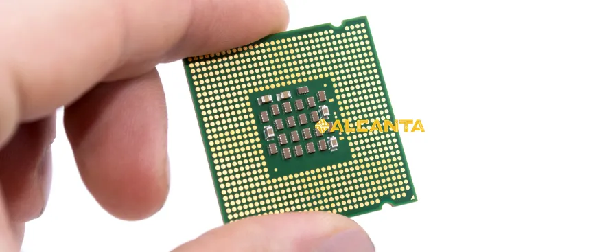
Semiconductor packaging technology has undergone a remarkable evolution, from traditional single-layer designs to the cutting-edge 3D chip packaging of today. Initially, chips were housed in simple packages to provide electrical connections and protect them from environmental factors. However, as demands for smaller, faster, and more powerful devices grew, innovative packaging solutions emerged.
Enter 3D chip packaging, a revolutionary approach that stacks multiple ICs vertically to maximize performance and density while minimizing footprint. This breakthrough technology represents a paradigm shift in semiconductor design, offering unparalleled levels of integration and functionality. Its significance in the industry cannot be overstated, as it paves the way for next-generation electronics across a multitude of applications, from mobile devices to data centers. In this blog, we’ll delve deeper into the realm of 3D chip packaging and explore its transformative impact on semiconductor innovation.
Understanding 3D Semiconductor Packaging:
Definition of 3D Semiconductor Packaging:
3D semiconductor packaging is a cutting-edge technology that involves vertically stacking multiple integrated circuits (ICs) on top of each other within a single package. Unlike traditional 2D packaging, which lays out ICs side by side, 3D packaging utilizes vertical space to enhance performance and functionality while minimizing footprint.
Explanation of Stacking Multiple Integrated Circuits Vertically:
In 3D semiconductor packaging, ICs are interconnected using advanced through-silicon via (TSV) technology, enabling vertical integration. This vertical stacking allows for closer proximity between different functional blocks, reducing interconnect lengths and enabling faster data transfer rates. Additionally, it facilitates heterogeneous integration, allowing different types of ICs, such as processors, memory, and sensors, to be stacked together for optimized system performance.
Highlighting the Benefits:
1. Improved Performance: By stacking ICs vertically, 3D packaging reduces interconnect lengths and parasitic capacitance, leading to faster signal propagation and lower power consumption. This results in enhanced overall system performance and efficiency.
2. Reduced Footprint: Traditional 2D packaging often requires larger form factors to accommodate all necessary components. 3D packaging, on the other hand, enables higher component density within a smaller footprint, making it ideal for compact electronic devices such as smartphones, wearables, and IoT devices.
3. Enhanced Functionality: The vertical integration of ICs allows for the creation of more complex and feature-rich systems. With 3D packaging, manufacturers can incorporate diverse functionalities, such as heterogeneous integration of different technologies (e.g., logic, memory, sensors), advanced power management, and system-in-package (SiP) solutions, all within a single package.
In summary, 3D semiconductor packaging revolutionizes the way electronic systems are designed and manufactured, offering unparalleled performance, compactness, and functionality. Its adoption is driving innovation across a wide range of industries, from consumer electronics to automotive and healthcare, paving the way for the next generation of high-performance computing and IoT devices.
Exploring the Difference Between 3D and 2.5D Packaging:
Definition and Explanation of 2.5D Packaging:
2.5D packaging, also known as 2.5D interposer technology, involves mounting multiple ICs onto a silicon interposer substrate, which acts as a bridge between the chips and the package substrate. Unlike traditional 2D packaging, where ICs are placed side by side on a single substrate, 2.5D packaging allows for higher component density and improved electrical performance by leveraging the interposer’s shorter interconnects.
Comparison between 3D and 2.5D Packaging Technologies:
1. Architecture: In 3D packaging, ICs are stacked vertically, allowing for direct connections between layers using through-silicon vias (TSVs). On the other hand, 2.5D packaging utilizes a silicon interposer to connect multiple ICs placed side by side, enabling shorter interconnect lengths but without the vertical stacking found in 3D packaging.
2. Complexity: 3D packaging typically involves more intricate fabrication processes, such as TSV formation and thinning of individual ICs, compared to 2.5D packaging. As a result, 3D packaging may be more challenging and costly to implement, but it offers greater integration density and performance benefits.
3. Applications: 3D packaging is well-suited for applications requiring ultra-compact form factors and high performance, such as advanced computing, artificial intelligence (AI), and high-bandwidth memory (HBM) applications. 2.5D packaging, on the other hand, is often used in applications where improved electrical performance and moderate integration density are desired, such as high-end graphics processing units (GPUs), networking, and server applications.
Illustration of Market Needs and Challenges Addressed by Each Technology:
3D Packaging: Addresses the growing demand for miniaturization and performance enhancement in portable electronics, IoT devices, and high-performance computing systems. Challenges include manufacturing complexity, thermal management, and ensuring reliability of TSVs.
2.5D Packaging: Meets the need for improved electrical performance and integration density in high-speed communication and data processing applications. Challenges include optimizing signal integrity on the silicon interposer, managing power dissipation, and addressing potential substrate warpage issues.
In essence, while both 3D and 2.5D packaging technologies offer significant advantages over traditional 2D packaging, they cater to different market segments and application requirements. Understanding the distinctions between these technologies is crucial for semiconductor designers and manufacturers to select the most suitable packaging solution for their specific needs.
Delving into Chip Packaging Technology:
Definition of Chip Packaging Technology:
Chip packaging technology involves the process of encapsulating semiconductor chips within protective casings and providing electrical connections to external components. This encapsulation not only shields the delicate silicon from environmental factors but also facilitates electrical connections for integration into larger electronic systems.
Overview of Different Chip Packaging Techniques:
1. Flip Chip Packaging: In flip chip packaging, the semiconductor die is flipped upside down and directly bonded to the substrate or interconnect using solder bumps. This approach offers high electrical performance, shorter interconnect lengths, and improved thermal management. It is commonly used in high-performance computing, mobile devices, and automotive electronics.
2. Monolithic 3D Packaging: Monolithic 3D packaging involves stacking multiple layers of active devices (transistors) vertically within a single silicon substrate. This technology enables dense integration of logic, memory, and other functionalities, resulting in improved performance and reduced power consumption. Monolithic 3D is particularly well-suited for applications requiring high-density memory and logic integration, such as data centers and AI accelerators.
3. Interposer-based Packaging: Interposer-based packaging utilizes a silicon interposer, a thin substrate with through-silicon vias (TSVs), to connect multiple chips or dies. The interposer acts as a bridge between the chips and the package substrate, enabling shorter interconnect lengths and improved signal integrity. This packaging technique is commonly used in 2.5D and 3D packaging solutions for high-performance computing, networking, and graphics applications.
Discussion on the Importance of Chip Packaging:
Chip packaging plays a critical role in ensuring the functionality, performance, and reliability of semiconductor devices. Some key points highlighting its importance include:
Protection: Packaging provides physical protection to the delicate semiconductor die from environmental factors such as moisture, dust, and mechanical stress.
Electrical Connections: Packaging facilitates electrical connections between the semiconductor die and external components, enabling seamless integration into electronic systems.
Thermal Management: Effective chip packaging helps dissipate heat generated during operation, preventing thermal issues that can degrade performance and reliability.
Signal Integrity: Proper packaging design minimizes signal distortion and electromagnetic interference, ensuring robust communication between integrated circuits.
Reliability: Well-designed chip packaging enhances the overall reliability and lifespan of semiconductor devices, meeting stringent quality and durability requirements for various applications.
In summary, chip packaging technology is essential for realizing the full potential of semiconductor devices, enabling them to meet the performance, reliability, and integration demands of modern electronic systems. Different packaging techniques offer unique advantages and cater to diverse application requirements, driving innovation in the semiconductor industry.
Unraveling the World of 3D Chips:
Definition and Characteristics of 3D Chips:
3D chips are semiconductor devices that utilize vertical stacking of multiple integrated circuits (ICs) to achieve enhanced performance, density, and functionality. Unlike traditional 2D chips, which are laid out side by side on a single plane, 3D chips leverage through-silicon via (TSV) technology to stack ICs vertically, creating a three-dimensional structure. This vertical integration allows for closer proximity between different functional blocks, shorter interconnect lengths, and improved signal propagation, leading to higher performance and efficiency.
Key characteristics of 3D chips include:
Vertical Integration: Stacking multiple ICs vertically within a single package or substrate.
Through-Silicon Vias (TSVs): Vertical interconnects that enable electrical connections between different layers of the 3D chip.
Heterogeneous Integration: Integration of diverse functionalities, such as processors, memory, sensors, and RF components, within a compact form factor.
Improved Performance: Reduced interconnect lengths and enhanced signal integrity result in faster data transfer rates and lower power consumption.
Compact Size: Achieving higher component density within a smaller footprint, making 3D chips ideal for space-constrained applications.
Explanation of How 3D Chip Stacking Enables Integration of Diverse Functionalities:
3D chip stacking facilitates the integration of diverse functionalities by allowing different types of ICs to be stacked on top of each other within a single package or substrate. For example, a 3D chip could include layers of logic ICs, memory ICs, and sensor ICs, all interconnected through TSVs. This heterogeneous integration enables the creation of highly integrated systems-on-chip (SoCs) with optimized performance, functionality, and power efficiency. Additionally, 3D chip stacking enables the co-design of different components, leading to synergistic interactions and enhanced system-level capabilities.
Showcase of Real-World Applications and Industries Benefiting from 3D Chip Technology:
1. Data Centers: 3D chips are revolutionizing the data center industry by enabling higher performance and energy efficiency in server processors, memory modules, and networking accelerators.
2. Consumer Electronics: Smartphones, tablets, and wearables benefit from 3D chip technology by achieving slimmer designs, longer battery life, and improved processing capabilities.
3. Automotive: 3D chips are used in advanced driver assistance systems (ADAS), infotainment systems, and autonomous vehicles to support real-time processing, sensor fusion, and connectivity.
4. Medical Devices: Medical imaging equipment, wearable health monitors, and implantable devices leverage 3D chip technology to improve diagnostic accuracy, data processing speed, and patient outcomes.
5. Telecommunications: 3D chips enable higher bandwidth, lower latency, and increased network capacity in 5G infrastructure, routers, and optical communication systems.
In summary, 3D chip technology is driving innovation across a wide range of industries, enabling the development of next-generation electronic devices with unprecedented levels of performance, functionality, and integration. Its ability to stack multiple ICs vertically opens up new possibilities for compact, efficient, and powerful semiconductor solutions.
Introducing Cadence Integrity 3D-IC:
Overview of Cadence Integrity 3D-IC Solution:
Cadence Integrity 3D-IC is a comprehensive design and verification solution tailored specifically for the development of advanced 3D integrated circuits (ICs). It provides a complete suite of tools and methodologies to address the unique challenges associated with 3D chip stacking, such as TSV design, thermal management, signal integrity, and system-level integration.
Highlighting its Features and Capabilities:
1. TSV Design and Optimization: Cadence Integrity 3D-IC offers advanced capabilities for designing and optimizing through-silicon vias (TSVs), including TSV placement, routing, and electrical modeling. This ensures robust TSV designs that meet performance, reliability, and manufacturability requirements.
2. Thermal Analysis: The solution includes thermal analysis tools to predict and mitigate thermal issues in 3D ICs, such as hot spots and thermal gradients. This enables designers to optimize thermal management strategies, such as TSV distribution and heat dissipation mechanisms, to prevent thermal-induced failures and ensure long-term reliability.
3. Signal Integrity and Power Integrity: Cadence Integrity 3D-IC provides comprehensive signal integrity and power integrity analysis tools to ensure reliable communication and power delivery within the stacked ICs. This includes simulation and optimization of signal propagation, impedance matching, and power distribution networks to minimize noise, crosstalk, and voltage drop issues.
4. System-Level Integration: The solution enables seamless integration of diverse functional blocks, such as logic, memory, and analog circuits, within a 3D IC. It includes tools for system-level co-design, partitioning, and verification to optimize performance, power, and area trade-offs across the entire chip stack.
Case Studies or Success Stories:
1. Accelerating Time-to-Market: A leading semiconductor company utilized Cadence Integrity 3D-IC to design and verify a complex 3D memory stacking solution for next-generation mobile devices. By leveraging the solution’s advanced TSV optimization and thermal analysis capabilities, the company reduced design iterations and accelerated time-to-market by 30%.
2. Optimizing Chip Performance: A networking equipment manufacturer deployed Cadence Integrity 3D-IC to develop a high-performance 3D chip solution for data center switches. Through comprehensive signal integrity and power integrity analysis, the manufacturer optimized the chip’s interconnect architecture and power delivery network, resulting in a 20% improvement in data transmission rates and power efficiency.
3. Ensuring Reliability: An automotive electronics supplier utilized Cadence Integrity 3D-IC to design a 3D IC for automotive radar systems. By simulating and optimizing thermal management strategies, such as TSV placement and heat dissipation mechanisms, the supplier ensured reliable operation of the radar system under harsh environmental conditions, such as high temperatures and vibration.
In conclusion, Cadence Integrity 3D-IC provides a comprehensive solution for designing and verifying advanced 3D integrated circuits, enabling semiconductor companies to accelerate time-to-market, optimize chip performance, and ensure reliability in a wide range of applications. Its advanced features and capabilities make it an indispensable tool for realizing the full potential of 3D chip technology.
FAQs about 3d chip packaging
3D semiconductor packaging involves vertically stacking multiple integrated circuits (ICs) within a single package or substrate. This innovative approach enables higher performance, density, and functionality by leveraging through-silicon via (TSV) technology to connect different layers of the chip stack.
The main difference between 3D and 2.5D packaging lies in their architecture and level of integration. In 3D packaging, ICs are stacked vertically, allowing direct connections between layers using TSVs. In contrast, 2.5D packaging involves mounting multiple ICs onto a silicon interposer substrate, which acts as a bridge between the chips. While both offer improved performance and density compared to traditional 2D packaging, 3D packaging provides greater integration and compactness by stacking ICs vertically.
Chip packaging technology encompasses the processes involved in encapsulating semiconductor chips within protective casings and providing electrical connections to external components. It ensures the functionality, reliability, and performance of semiconductor devices by shielding them from environmental factors, facilitating electrical connections, managing thermal dissipation, and optimizing signal integrity.
3D chips are semiconductor devices that leverage vertical stacking of multiple ICs to achieve enhanced performance, density, and functionality. These chips feature through-silicon vias (TSVs) for vertical interconnections between different layers, enabling closer proximity between functional blocks, shorter interconnect lengths, and improved signal propagation.


发表评论
Want to join the discussion?Feel free to contribute!