
Understanding Package Substrate Materials for Modern Electronics
Package substrates play a crucial role in modern electronics, serving as the foundational layer that supports and interconnects various components within a device. Their importance lies in their ability to enhance electrical performance, provide mechanical stability, and enable miniaturization of electronic products. As the demand for more compact and efficient devices grows, package substrates become increasingly vital in achieving these advancements.
In electronic products, package substrates are used extensively in integrated circuits (ICs), microelectromechanical systems (MEMS), and advanced sensor technologies. They facilitate high-density interconnections, improve signal integrity, and support thermal management, making them indispensable in industries such as consumer electronics, automotive, telecommunications, and healthcare.
This article will delve into the definition and functions of package substrates, explore embedded trace substrates, discuss the process and importance of IC packaging and testing, and examine the differences between package substrates and printed circuit boards (PCBs). Additionally, we will cover the various materials used for package substrates and their significance, as well as future development trends in this critical field.
Definition of Package Substrate
What is a Package Substrate?
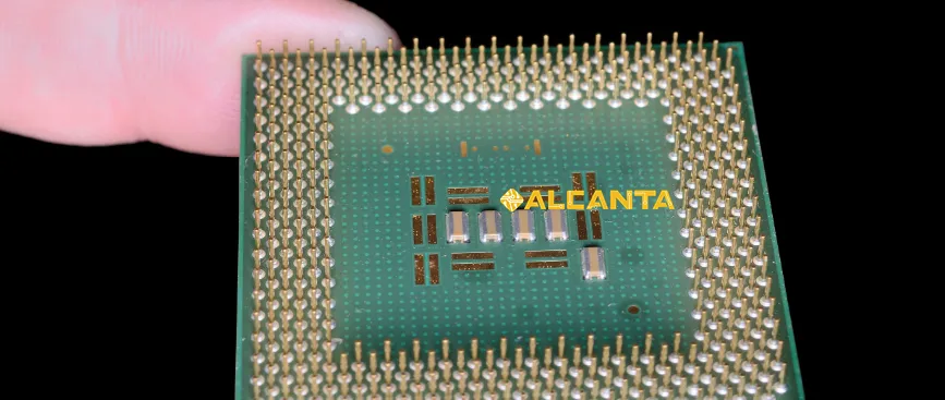
A package substrate is a crucial component in semiconductor packaging, serving as the physical foundation that supports and interconnects the semiconductor die to the rest of the electronic system. It is typically composed of multiple layers of organic or inorganic materials, including metals, ceramics, and polymers, designed to facilitate electrical connections, mechanical support, and heat dissipation. Package substrates come in various forms, such as single-layer, multilayer, and embedded trace substrates, each tailored to specific applications and performance requirements.
Functions and Roles of Package Substrates
Electrical Interconnection
One of the primary functions of a package substrate is to provide electrical interconnections between the semiconductor die and the external circuitry. This is achieved through a network of conductive traces, vias, and pads that form the pathways for electrical signals. These interconnections ensure that signals are transmitted with minimal loss and interference, enhancing the overall performance of the electronic device.
Mechanical Support
Package substrates also provide mechanical support and protection for the delicate semiconductor die. By securing the die in place and shielding it from physical damage, substrates help maintain the integrity and reliability of the device. The substrate’s rigidity and stability are essential for ensuring that the die remains securely attached and functions correctly over its lifetime.
Thermal Management
Effective thermal management is critical in electronic devices to prevent overheating and ensure optimal performance. Package substrates play a vital role in dissipating heat generated by the semiconductor die during operation. They are designed with materials and structures that enhance heat transfer away from the die, thereby maintaining the device’s temperature within safe limits and prolonging its operational life.
Miniaturization and Integration
As the demand for smaller and more compact electronic devices increases, package substrates enable the miniaturization and integration of multiple components into a single package. Advanced substrate technologies, such as embedded trace substrates, allow for higher density interconnections and more efficient use of space. This leads to the development of more powerful and feature-rich electronic products without increasing their size.
Signal Integrity and Performance
High-frequency and high-speed applications require substrates that can maintain signal integrity and performance. Package substrates are engineered to minimize signal loss, crosstalk, and electromagnetic interference, ensuring that the electronic device operates reliably and efficiently. The design and material selection of the substrate are crucial in achieving these performance characteristics.
In summary, package substrates are indispensable in modern electronics, providing the necessary support, interconnections, and thermal management required for the efficient and reliable operation of semiconductor devices. Their role in enabling miniaturization and maintaining signal integrity underscores their importance in the ongoing advancement of electronic technology.
Embedded Trace Substrate
Concept of Embedded Trace Substrates
Embedded trace substrates (ETS) represent a significant advancement in substrate technology, incorporating conductive traces within the layers of the substrate rather than on the surface. This innovative approach allows for a more compact and efficient design, enhancing the performance and reliability of electronic devices. The traces are embedded within the substrate material, typically made of organic or inorganic compounds, and are interconnected through vertical vias that allow electrical signals to pass between different layers. This configuration not only saves space but also provides better protection for the conductive paths, reducing the risk of damage and improving overall device durability.
Advantages of Embedded Trace Substrates
Space Efficiency and Miniaturization
One of the most notable advantages of embedded trace substrates is their ability to significantly reduce the overall size of electronic packages. By embedding the traces within the substrate layers, more circuitry can be packed into a smaller area, enabling the design of smaller and more compact electronic devices. This is particularly beneficial in applications where space is at a premium, such as in smartphones, wearables, and other portable electronics.
Enhanced Electrical Performance
Embedded trace substrates offer superior electrical performance compared to traditional surface-mounted traces. The embedded configuration reduces inductance and resistance, resulting in lower signal loss and improved signal integrity. This is crucial for high-speed and high-frequency applications where maintaining signal quality is essential. The reduced electrical path length also helps minimize delay, further enhancing the device’s performance.
Improved Reliability and Durability
The traces embedded within the substrate are better protected from environmental factors such as moisture, contaminants, and physical stress. This enhances the reliability and longevity of the electronic device. The encapsulation of traces within the substrate also reduces the risk of trace damage during handling and assembly, contributing to improved product durability and reduced failure rates.
Better Thermal Management
Embedded trace substrates facilitate better thermal management by distributing heat more evenly across the substrate layers. This helps in maintaining a consistent temperature, preventing hotspots, and enhancing the overall thermal performance of the device. Effective thermal management is critical in high-power applications to ensure the device operates within safe temperature limits and prolongs its operational life.
Applications of Embedded Trace Substrates
High-Density Interconnect (HDI) Boards
Embedded trace substrates are widely used in high-density interconnect (HDI) boards, which require a high level of miniaturization and performance. These boards are commonly found in advanced electronics such as smartphones, tablets, and laptops, where space constraints and performance demands are significant.
Automotive Electronics
In the automotive industry, embedded trace substrates are used in advanced driver-assistance systems (ADAS), infotainment systems, and engine control units. The ability to provide reliable performance in harsh environments makes ETS ideal for automotive applications where durability and performance are critical.
Medical Devices
Medical devices, particularly those used in diagnostic and monitoring equipment, benefit from the compact and reliable nature of embedded trace substrates. The miniaturization capability of ETS allows for the development of smaller, portable medical devices that can deliver high performance and reliability.
Aerospace and Defense
The aerospace and defense sectors utilize embedded trace substrates in applications where reliability and performance under extreme conditions are paramount. The robustness and enhanced electrical performance of ETS make them suitable for use in avionics, satellite communications, and military equipment.
In conclusion, embedded trace substrates offer numerous advantages that make them ideal for a wide range of high-performance, high-reliability applications. Their ability to support miniaturization, improve electrical performance, and enhance durability and thermal management underscores their importance in the evolution of advanced electronic technologies.
IC Packaging and Testing
Process and Technology of IC Packaging
IC Packaging Process
The IC packaging process involves several key steps to encase and protect integrated circuits (ICs), while ensuring reliable electrical and mechanical connections to the external circuitry. The process typically starts with the preparation of the semiconductor die, which is then mounted onto a package substrate. The die is connected to the substrate using wire bonding or flip-chip techniques, depending on the package type. After the die is secured, the package is encapsulated with a protective material, such as epoxy or plastic molding, to shield it from environmental factors and mechanical stress. Finally, the package undergoes various tests to ensure it meets performance and reliability standards before it is ready for integration into electronic devices.
Packaging Technologies
Several packaging technologies are employed based on the specific requirements of the IC and its application. Common technologies include:
– Wire Bonding: A traditional method where fine wires connect the die’s bonding pads to the package leads or substrate.
– Flip-Chip Technology: The die is flipped and mounted directly onto the substrate, with solder bumps providing electrical connections. This method allows for higher performance and miniaturization.
– Ball Grid Array (BGA): ICs are mounted on a substrate with an array of solder balls that serve as electrical and mechanical connections. BGAs offer high pin density and improved thermal performance.
– Chip-On-Board (COB): The die is directly attached to a printed circuit board (PCB) and wire-bonded to the board’s circuitry. This method is used for cost-effective and compact applications.
Importance of IC Testing
Ensuring Reliability and Performance
IC testing is crucial to verify that the packaged ICs meet the required performance and reliability standards. Testing helps identify defects or anomalies that could affect the functionality of the IC or the overall device. Comprehensive testing ensures that the IC performs reliably under various conditions, including temperature fluctuations, electrical stress, and mechanical forces. This helps prevent potential failures that could lead to device malfunctions or reduced lifespan.
Detecting Manufacturing Defects
Manufacturing defects can arise from various sources, including material inconsistencies, process variations, or handling issues. IC testing helps detect these defects early in the production cycle, allowing for corrective actions to be taken before the ICs are shipped to customers. This helps maintain high-quality standards and reduces the risk of costly returns or recalls.
Validating Performance Specifications
IC testing verifies that the ICs meet their specified performance parameters, such as speed, power consumption, and signal integrity. Testing ensures that the IC operates within its intended performance range and meets the requirements of its target application. This validation is critical for maintaining the integrity of the end product and meeting customer expectations.
Role of Package Substrates in IC Packaging and Testing
Electrical Interconnections
Package substrates play a vital role in facilitating electrical connections between the IC die and the external circuitry. The substrate provides the conductive pathways required for signal transmission and power distribution. The design and quality of the package substrate directly impact the performance of the IC, influencing factors such as signal integrity, electrical resistance, and heat dissipation.
Mechanical Support and Protection
The package substrate provides mechanical support for the IC die, ensuring that it remains securely attached and protected during operation and handling. This support is essential for preventing damage to the delicate die and maintaining the integrity of the electrical connections. The substrate also shields the die from environmental factors and physical stress, contributing to the overall reliability of the packaged IC.
Thermal Management
Effective thermal management is critical for maintaining the performance and longevity of ICs. Package substrates are designed to enhance heat dissipation from the die, preventing overheating and ensuring stable operation. Advanced substrates incorporate thermal vias, heat spreaders, and other features to manage heat effectively, which is crucial for high-power and high-performance applications.
Integration with Testing Systems
Package substrates must be compatible with testing systems used to evaluate the ICs. The design of the substrate affects the accessibility of test points and the ease of interfacing with testing equipment. Proper integration of the package substrate with testing systems ensures accurate and efficient testing, facilitating the identification of potential issues and ensuring that only high-quality ICs reach the market.
In summary, IC packaging and testing are integral to the development of reliable and high-performance semiconductor devices. The process and technology of IC packaging ensure that ICs are securely encased and connected, while testing verifies their functionality and quality. Package substrates play a crucial role in both packaging and testing, providing electrical interconnections, mechanical support, and thermal management essential for the successful operation of integrated circuits.
IC Substrate
What is an IC Substrate?
An IC substrate is a specialized type of substrate used to support and interconnect integrated circuits (ICs) within electronic devices. It serves as the foundation upon which the IC is mounted and connected to the external circuitry. IC substrates are designed to provide mechanical support, electrical interconnections, and thermal management for the IC, ensuring its proper function and reliability. These substrates are made from various materials, including organic laminates, ceramics, and metals, depending on the specific requirements of the application.
IC substrates typically consist of multiple layers, including conductive layers for electrical connections, insulating layers to prevent electrical shorts, and sometimes thermal dissipation layers to manage heat. They are engineered to handle high-density interconnections, support high-speed signals, and provide durability under various operating conditions.
Characteristics of IC Substrates
Electrical Performance
IC substrates are designed to ensure high electrical performance by providing low resistance and low inductance paths for signal transmission. This is crucial for maintaining signal integrity and reducing crosstalk, especially in high-speed and high-frequency applications. The choice of materials and the design of the conductive layers play a significant role in achieving optimal electrical performance.
Mechanical Strength and Stability
The mechanical strength of an IC substrate is essential for protecting the delicate IC die and maintaining its alignment with the external circuitry. The substrate must be rigid and stable to prevent mechanical stress that could lead to die shift or damage. Materials used in IC substrates, such as high-strength ceramics or reinforced organic laminates, contribute to their mechanical durability.
Thermal Management
Effective thermal management is a key characteristic of IC substrates, as they help dissipate heat generated by the IC during operation. Substrates are designed with thermal vias, heat spreaders, or heat sinks to facilitate heat transfer away from the IC, preventing overheating and ensuring stable performance. The thermal conductivity of the substrate material is a critical factor in managing heat effectively.
Size and Form Factor
IC substrates are available in various sizes and form factors to accommodate different IC packages and applications. The substrate’s size and shape must match the requirements of the IC and the overall design of the electronic device. Advanced substrates may offer flexibility in form factors to support compact and complex designs.
Reliability and Durability
Reliability and durability are essential characteristics of IC substrates, as they must withstand environmental factors such as temperature fluctuations, humidity, and mechanical stress. High-quality substrates are designed to maintain their performance and integrity over the long term, ensuring the longevity of the electronic device.
Application Fields of IC Substrates
5.3.1 Consumer Electronics
IC substrates are widely used in consumer electronics, including smartphones, tablets, and laptops. These applications require high-density interconnections, excellent electrical performance, and compact designs. IC substrates in consumer electronics support various functions such as processing, memory, and communication, enabling advanced features and high performance.
Automotive Electronics
In the automotive industry, IC substrates are used in applications such as advanced driver-assistance systems (ADAS), infotainment systems, and engine control units. Automotive electronics demand high reliability and performance under harsh conditions, making IC substrates with robust mechanical and thermal properties essential for ensuring safety and functionality.
Medical Devices
IC substrates are critical in medical devices, including diagnostic equipment, monitoring systems, and imaging systems. These applications require high precision, reliability, and compactness. IC substrates in medical devices support sensitive electronics that need to perform accurately and consistently in demanding environments.
Aerospace and Defense
The aerospace and defense sectors utilize IC substrates in avionics, satellite communications, and military systems. These applications often involve extreme conditions, such as high temperatures, vibrations, and radiation. IC substrates used in these fields must offer superior durability, thermal management, and performance to ensure reliable operation in challenging environments.
Telecommunications
In telecommunications, IC substrates support high-speed communication equipment, including network switches, routers, and base stations. These applications require substrates that can handle high-frequency signals, provide reliable connections, and manage heat effectively to maintain performance and system stability.
In summary, IC substrates are vital components in modern electronic devices, providing essential support, electrical connections, and thermal management for integrated circuits. Their characteristics, including electrical performance, mechanical strength, thermal management, size, and reliability, are tailored to meet the demands of various application fields, from consumer electronics to aerospace and defense.
Difference Between Package Substrate and Printed Circuit Board (PCB)
Definition and Structural Differences
Definition of Package Substrate
A package substrate is a specialized type of substrate designed to support and interconnect integrated circuits (ICs) within an electronic package. It provides the necessary electrical connections between the IC die and the external circuitry, and also offers mechanical support and thermal management. Package substrates are typically multi-layer structures, incorporating conductive traces, insulating layers, and sometimes thermal vias or heat spreaders. They are designed to handle high-density interconnections and are used primarily within the context of semiconductor packaging.
Definition of Printed Circuit Board (PCB)
A printed circuit board (PCB) is a broader category of substrate used to mechanically support and electrically connect various electronic components within a device. PCBs are typically single-sided, double-sided, or multi-layered boards with conductive pathways (traces) etched onto a dielectric material. They are used in a wide range of electronic devices, from simple consumer gadgets to complex industrial systems. PCBs serve as the foundational platform for mounting and interconnecting electronic components, providing the necessary pathways for electrical signals and power.
Structural Differences
– Layers and Complexity: Package substrates are often more complex and can have multiple layers, including embedded traces and vias for high-density interconnections. In contrast, PCBs can vary from simple single-layer designs to complex multi-layer constructions, but they generally do not feature the same level of integration as package substrates.
– Conductive Paths: In package substrates, conductive paths are often embedded within the substrate layers, which enhances space efficiency and protects the traces. PCBs typically have conductive traces on the surface or within layers that are visible and accessible.
– Materials: Package substrates often use advanced materials, such as high-performance ceramics or specialized organic laminates, to meet specific electrical, thermal, and mechanical requirements. PCBs use a variety of materials ranging from standard FR-4 laminates to high-frequency materials, depending on the application.
– Thermal Management: Package substrates are designed with advanced thermal management features, such as heat spreaders or thermal vias, to handle heat dissipation from high-performance ICs. PCBs may include some thermal management features but generally focus more on supporting component mounting and electrical connectivity.
Comparison of Application Scenarios
Package Substrate Applications
– High-Performance ICs: Package substrates are used in applications requiring high-density interconnections and high-performance ICs, such as advanced processors, memory modules, and RF components. They provide the necessary support and connectivity for complex semiconductor devices.
– Consumer Electronics: In consumer electronics, such as smartphones and tablets, package substrates support various high-speed and high-density ICs, ensuring reliable performance and compact design.
– Automotive Electronics: Package substrates are used in automotive electronics for critical systems like advanced driver-assistance systems (ADAS) and engine control units (ECUs), where reliability and thermal management are crucial.
– Medical Devices: In medical devices, package substrates are used to support sensitive and high-precision ICs, ensuring accurate performance and durability in diagnostic and monitoring equipment.
PCB Applications
– General Electronics: PCBs are used in a wide range of general electronics applications, including consumer devices, industrial equipment, and home appliances. They provide the foundation for mounting and interconnecting various electronic components.
– Prototyping and Development: PCBs are commonly used for prototyping and development purposes due to their versatility and ease of fabrication. They allow engineers to design and test electronic circuits before finalizing the product.
– Low to Mid-Complexity Devices: PCBs are suitable for devices with lower to mid-level complexity, where the primary focus is on providing reliable electrical connections and mechanical support rather than high-density interconnections.
– Signal and Power Distribution: PCBs are used for signal and power distribution in a variety of applications, from power supplies to communication systems, where standard connectivity and signal routing are sufficient.
In summary, while both package substrates and PCBs are essential in electronic systems, they serve different roles and are optimized for different applications. Package substrates are specialized for high-density, high-performance IC packaging with advanced thermal management, whereas PCBs are more versatile and widely used for general electrical connections and support across a broad range of electronic devices.
Package Substrate Materials
Common Types of Package Substrate Materials
Organic Laminates
Organic laminates, such as those based on epoxy resin or polyimide, are commonly used in package substrates. These materials provide a flexible and cost-effective solution for various applications. Organic laminates are made from layers of reinforcing fibers and resin, which are laminated together to form a substrate with embedded conductive traces.
Ceramics
Ceramic substrates, including alumina (Al2O3) and aluminum nitride (AlN), are used for their excellent thermal conductivity and mechanical strength. Ceramics are particularly suited for high-power and high-frequency applications where thermal management is critical. These substrates offer superior performance in heat dissipation and reliability under extreme conditions.
Metal-Based Substrates
Metal-based substrates, such as those with copper or aluminum cores, are designed to provide enhanced thermal conductivity. These substrates typically feature a metal core layer that helps dissipate heat away from the IC. They are often used in applications where high thermal performance is required, such as power electronics and LED lighting.
High-Frequency Materials
High-frequency materials, such as those with PTFE (polytetrafluoroethylene) or other advanced polymers, are used in substrates designed for RF (radio frequency) and microwave applications. These materials have low dielectric constants and low loss tangents, which help maintain signal integrity at high frequencies.
Analysis of the Characteristics and Advantages/Disadvantages of Each Material
Organic Laminates
– Characteristics: Organic laminates offer flexibility, ease of fabrication, and cost-effectiveness. They are commonly used in a wide range of consumer and industrial applications.
– Advantages:
– Cost-effective and widely available.
– Suitable for high-density interconnections and complex designs.
– Good mechanical properties and ease of processing.
– Disadvantages:
– Lower thermal conductivity compared to ceramics and metal-based substrates.
– Limited performance in extreme temperatures and high-frequency applications.
7.2.2 Ceramics
– Characteristics: Ceramic substrates provide high thermal conductivity, mechanical strength, and stability. They are ideal for applications requiring efficient heat dissipation and reliable performance.
– Advantages:
– Excellent thermal conductivity and heat dissipation.
– High mechanical strength and durability.
– Stable performance under high temperatures and harsh environments.
– Disadvantages:
– Higher cost compared to organic laminates.
– Brittle nature can make them prone to mechanical damage.
– More complex and expensive to manufacture and process.
Metal-Based Substrates
– Characteristics: Metal-based substrates, such as those with aluminum or copper cores, are designed for superior thermal management. They are particularly useful in high-power and high-thermal applications.
– Advantages:
– Excellent thermal conductivity and heat dissipation.
– Effective in managing heat in power electronics and LEDs.
– Robust mechanical properties.
– Disadvantages:
– Higher cost compared to organic laminates.
– Heavier and more rigid, which can limit design flexibility.
– Processing and manufacturing can be more complex.
High-Frequency Materials
– Characteristics: High-frequency materials are engineered for low loss and high signal integrity in RF and microwave applications. They are used where maintaining signal quality at high frequencies is essential.
– Advantages:
– Low dielectric constant and low loss tangent for minimal signal degradation.
– Ideal for high-frequency and high-speed applications.
– Can handle high-frequency signal routing effectively.
– Disadvantages:
– Typically more expensive than standard materials.
– Limited mechanical strength and durability compared to ceramics and metals.
– Specialized processing and handling requirements.
Key Factors in Material Selection
Thermal Performance
The thermal performance of a package substrate material is crucial for applications involving high power or high-frequency components. Materials with high thermal conductivity, such as ceramics and metal-based substrates, are preferred for efficient heat dissipation and thermal management.
Electrical Performance
The material’s electrical properties, including dielectric constant and loss tangent, impact signal integrity and performance. For high-speed and high-frequency applications, materials with low dielectric constants and low loss tangents, such as high-frequency polymers, are essential.
Mechanical Properties
The mechanical strength and flexibility of the substrate material affect its durability and ability to support the IC. Considerations include the material’s resistance to mechanical stress, impact, and thermal cycling. Ceramics offer high strength, while organic laminates provide more flexibility.
Cost and Fabrication
Cost and ease of fabrication are significant factors in material selection. Organic laminates are cost-effective and widely used, while ceramics and metal-based substrates, though more expensive, provide enhanced performance for specific applications. The complexity of the manufacturing process also affects material choice.
Application Requirements
The specific requirements of the application, including operating temperature, environmental conditions, and mechanical constraints, guide the selection of the appropriate substrate material. Each material offers different advantages and trade-offs, making it essential to match the material properties with the application’s needs.
In conclusion, the selection of package substrate materials involves balancing factors such as thermal performance, electrical performance, mechanical properties, cost, and specific application requirements. By understanding the characteristics and advantages/disadvantages of each material, designers can choose the most suitable substrate to meet the demands of their electronic devices.
FAQs about package substrate material
A package substrate is a specialized material used to support and interconnect integrated circuits (ICs) within an electronic package. It provides mechanical support, electrical connections, and thermal management for the IC.
A PCB (printed circuit board) supports and connects various electronic components in a device, while a package substrate specifically supports and connects an IC to the external circuitry. Package substrates are typically more complex and focused on high-density interconnections and thermal management.
Common materials for substrates include organic laminates (e.g., epoxy resin), ceramics (e.g., alumina, aluminum nitride), metal-based materials (e.g., copper or aluminum cores), and high-frequency materials (e.g., PTFE).
In packaging, a substrate refers to the material layer that provides support and electrical connections for an integrated circuit within a package. It plays a critical role in connecting the IC to the external circuitry and managing heat.

