
Understanding the Critical Steps in Substrate Process Flow
In semiconductor manufacturing, a substrate refers to the base material upon which integrated circuits (ICs) are built. It serves as the foundation that supports and interconnects electronic components within the IC. The choice of substrate material significantly impacts the performance, reliability, and manufacturability of ICs. Substrates provide essential functions such as thermal dissipation, electrical insulation, and mechanical support, crucial for maintaining the integrity and longevity of electronic devices. Understanding substrate materials and their manufacturing processes is vital for optimizing IC performance and enabling advancements in semiconductor technology. This blog explores the intricate process flows involved in substrate manufacturing, along with comparisons between different bonding techniques and materials used in semiconductor packaging.
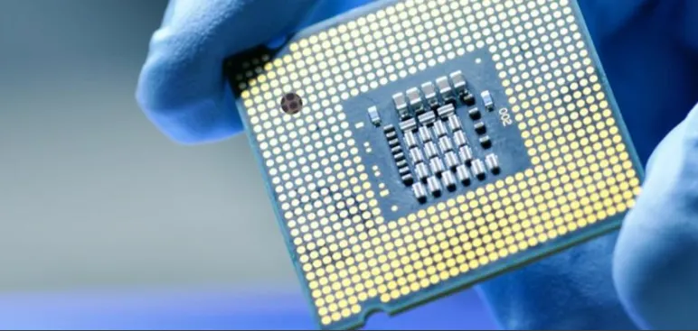
IC Substrate Manufacturing Process
Substrate Material Selection
In semiconductor manufacturing, choosing the right substrate material is crucial for the performance and reliability of integrated circuits (ICs). Two primary types of substrate materials commonly used are organic and ceramic.
- Organic Substrates: Made from materials like epoxy resins and polyimides, organic substrates are lightweight and cost-effective. They offer good electrical insulation and are suitable for high-speed applications.
- Ceramic Substrates: Typically composed of alumina (Al₂O₃) or aluminum nitride (AlN), ceramic substrates provide excellent thermal conductivity and mechanical strength. They are ideal for power devices and applications requiring efficient heat dissipation.
Factors influencing material choice include thermal conductivity, electrical properties (dielectric constant, impedance), mechanical strength, and cost-effectiveness.
Substrate Fabrication
Core Substrate Manufacturing Process
Layering and Lamination:
- Multiple layers of substrate material are laminated together using heat and pressure to form a solid base.
Copper Foil Application:
- Copper foil is bonded to the substrate surface through a process like electroplating or lamination.
Etching and Pattern Formation:
- Chemical etching techniques are employed to create circuit patterns on the substrate surface, defining the paths for electrical connections.
Via Drilling and Plating:
- Tiny holes (vias) are drilled through the substrate to connect different layers. These vias are then plated with conductive materials like copper to ensure electrical continuity.
Solder Mask Application:
- A protective layer (solder mask) is applied over the substrate surface, exposing only the areas where electrical connections (pads) will be made.
Build-up Substrate Manufacturing Process
Sequential Build-up (SBU) Process:
- Successive layers of dielectric materials and copper traces are added on top of the core substrate, creating complex multi-layered structures.
Laser Drilling and Copper Filling:
- High-precision lasers are used to drill vias in build-up layers, followed by copper filling to establish electrical pathways.
Dielectric and Resin Coating:
- Dielectric materials and resin coatings are applied between layers to insulate and protect conductive traces, ensuring signal integrity and reliability.
Surface Finish and Coating
Surface Finish Options:
- ENIG (Electroless Nickel Immersion Gold): Provides excellent oxidation resistance and solderability.
- OSP (Organic Solderability Preservatives): Protects copper surfaces and enhances solderability.
- HASL (Hot Air Solder Leveling): Ensures flat, solderable surfaces for component attachment.
Importance of Coatings in IC Performance:
- Surface finishes and coatings play a critical role in preventing corrosion, promoting solder joint reliability, and ensuring long-term performance of ICs in various environmental conditions.
This detailed overview highlights the intricate processes involved in IC substrate manufacturing, emphasizing the critical role of material selection, fabrication techniques, and surface treatments in achieving optimal semiconductor performance.
Comparison: Flip Chip vs. Wire Bonding
Flip Chip Bonding
Process Overview:
- Flip chip bonding involves placing the semiconductor die upside down and directly attaching it to the substrate or another die using solder bumps or conductive adhesives. This method eliminates the need for wire bonds by creating direct electrical connections through the solder bumps.
Advantages and Applications:
- Advantages:
- Higher Electrical Performance: Shorter interconnect paths reduce resistance and inductance, leading to better signal integrity and higher speed.
- Improved Thermal Management: Direct attachment allows for efficient heat dissipation, crucial for high-power devices.
- High Density and Miniaturization: Enables a higher density of interconnects, making it ideal for compact and complex designs.
- Reliability: Reduced mechanical stress and enhanced reliability compared to wire bonding.
- Applications:
- High-Performance Computing: Used in CPUs and GPUs where speed and performance are critical.
- Mobile Devices: Ideal for smartphones and tablets due to its compact size and efficient heat management.
- Advanced Packaging: Employed in multi-chip modules (MCM) and system-in-package (SiP) solutions.
Challenges and Limitations:
- Complex Manufacturing: Requires precise alignment and advanced equipment, increasing production complexity.
- Cost: Higher initial setup and material costs compared to wire bonding.
- Thermal Mismatch: Potential issues with thermal expansion differences between the die and substrate materials.
Wire Bonding
Process Overview:
- Wire bonding involves using fine wires (typically gold, aluminum, or copper) to connect the semiconductor die to the substrate or lead frame. The wires are bonded to the die and substrate through thermocompression, thermosonic, or ultrasonic welding techniques.
Advantages and Applications:
- Advantages:
- Simplicity and Cost-Effectiveness: Established and straightforward process with lower initial setup costs.
- Flexibility: Capable of connecting dies to various types of substrates and lead frames.
- Repairability: Easier to rework and repair compared to flip chip bonding.
- Applications:
- Consumer Electronics: Widely used in devices like TVs, radios, and household appliances.
- Automotive Electronics: Employed in sensors and control units where reliability and durability are essential.
- General IC Packaging: Commonly used in standard IC packages, such as dual in-line packages (DIP) and quad flat packages (QFP).
Challenges and Limitations:
- Electrical Performance: Longer interconnect paths can lead to higher resistance and inductance, affecting signal integrity and speed.
- Thermal Management: Less efficient heat dissipation compared to flip chip bonding.
- Mechanical Reliability: Wire bonds are more susceptible to mechanical stress and damage.
Comparison
Performance Metrics (speed, size, reliability):
- Speed: Flip chip bonding offers higher speed due to shorter interconnects and reduced parasitic effects. Wire bonding, with its longer wires, may experience slower signal transmission.
- Size: Flip chip enables more compact designs with higher interconnect density. Wire bonding typically requires more space due to the wire loops.
- Reliability: Flip chip bonding generally provides better mechanical and thermal reliability. Wire bonding, while simpler, may face issues with wire breakage and stress.
Suitability for Different Applications (high-speed vs. power devices):
- High-Speed Applications: Flip chip bonding is preferred for high-speed and high-frequency applications, such as processors and RF devices, due to its superior electrical performance.
- Power Devices: Both flip chip and wire bonding can be used, but flip chip’s better thermal management makes it suitable for high-power applications, while wire bonding remains common in cost-sensitive and less demanding power devices.
This detailed comparison highlights the distinct advantages, challenges, and applications of flip chip and wire bonding technologies, providing a comprehensive understanding of their roles in semiconductor packaging.
Differences Between Lead Frame and Substrate
Lead Frame
Definition and Purpose:
- A lead frame is a metal structure used in semiconductor packaging that provides the electrical connections between the semiconductor die and external circuitry. It acts as a framework to support and secure the semiconductor chip while enabling connections through wire bonding or other methods.
Manufacturing Process:
- Stamping: Lead frames are typically manufactured by stamping metal sheets (usually copper alloys or iron-nickel alloys) into precise shapes and dimensions using high-speed stamping machines.
- Plating: The stamped frames undergo plating with metals such as silver, nickel, or gold to enhance electrical conductivity and prevent oxidation.
- Assembly: The lead frame is then integrated with the semiconductor die and encapsulated in a protective package, such as plastic or ceramic.
Applications and Advantages:
- Applications: Lead frames are commonly used in a wide range of semiconductor packages, including dual in-line packages (DIP), small-outline packages (SOP), and quad flat packages (QFP).
- Advantages:
- Cost-Effective: Simple and cost-effective manufacturing process.
- Reliable: Proven technology with high reliability.
- Versatile: Suitable for various types of semiconductor devices and packaging styles.
- Thermal Performance: Good thermal conductivity due to the metal construction, aiding in heat dissipation.
Substrate
Definition and Role in Semiconductor Packaging:
- A substrate in semiconductor packaging refers to the base material on which integrated circuits (ICs) are built. It provides mechanical support, electrical connections, and thermal management for the semiconductor devices.
Manufacturing Process (as outlined in Section 1):
- Material Selection: Choosing between organic substrates (e.g., epoxy resins) and ceramic substrates (e.g., alumina).
- Core Substrate Manufacturing: Involves layering, lamination, copper foil application, etching, via drilling and plating, and solder mask application.
- Build-up Substrate Manufacturing: Adds layers sequentially through processes like laser drilling, copper filling, and dielectric/resin coating.
- Surface Finish: Applying surface finishes such as ENIG, OSP, or HASL to enhance solderability and protect against corrosion.
Applications and Advantages:
- Applications: Used in advanced semiconductor packages, including ball grid arrays (BGA), chip-scale packages (CSP), and flip-chip packages.
- Advantages:
- High Density: Supports high-density interconnections, making it ideal for complex and miniaturized designs.
- Electrical Performance: Superior electrical performance with lower inductance and resistance.
- Thermal Management: Efficient thermal management, especially with ceramic substrates.
- Flexibility: Versatile in accommodating various IC designs and advanced packaging technologies.
Comparison
Material Choices:
- Lead Frame: Typically made from metal alloys such as copper or iron-nickel.
- Substrate: Made from organic materials (e.g., epoxy resins) or ceramics (e.g., alumina, aluminum nitride).
Cost Considerations:
- Lead Frame: Generally more cost-effective due to simpler manufacturing processes and materials.
- Substrate: Higher cost associated with advanced materials and complex fabrication techniques, but provides better performance and miniaturization capabilities.
Performance Metrics (thermal dissipation, electrical connectivity):
- Thermal Dissipation: Lead frames have good thermal conductivity, making them suitable for applications requiring efficient heat dissipation. Substrates, particularly ceramic ones, offer superior thermal management for high-power and high-performance applications.
- Electrical Connectivity: Substrates provide better electrical performance with lower inductance and resistance, essential for high-speed and high-frequency applications. Lead frames, while reliable, have longer interconnect paths that can introduce higher resistance and inductance.
This detailed comparison highlights the distinct roles, manufacturing processes, applications, and advantages of lead frames and substrates in semiconductor packaging, providing a comprehensive understanding of their differences and respective benefits.
Advanced Topics: Coreless Substrate Process
Coreless Substrate
Definition and Benefits:
- Definition: A coreless substrate is a type of substrate used in semiconductor packaging that omits the traditional solid core layer found in conventional substrates. It relies on high-density interconnect (HDI) technology to create a stable and functional base for semiconductor devices.
- Benefits:
- Improved Electrical Performance: Eliminates the core, reducing parasitic capacitance and inductance, which enhances signal integrity and speed.
- Enhanced Thermal Management: Better heat dissipation due to the absence of a central core, which can act as a thermal barrier.
- Miniaturization: Allows for thinner and more compact packaging, essential for modern electronic devices.
- Flexibility: More design flexibility, enabling complex and dense interconnect patterns.
Manufacturing Challenges and Solutions
- Challenges:
- Precision in Layer Alignment: Ensuring accurate alignment of multiple layers without a central core to guide the process.
- Material Handling: Managing the thin and delicate materials used in coreless substrates can be difficult.
- Manufacturing Yield: Achieving high yield rates can be challenging due to the complexity and precision required.
- Reliability: Ensuring long-term reliability without the structural support of a core.
- Solutions:
- Advanced Manufacturing Techniques: Utilizing state-of-the-art equipment and robotics for precise layer stacking and alignment.
- Quality Control: Implementing rigorous quality control measures and real-time monitoring to detect and correct issues early in the process.
- Material Innovations: Developing new materials and adhesives that provide better stability and performance.
- Process Optimization: Continuous improvement of manufacturing processes to enhance yield and reliability.
Applications in Advanced Semiconductor Packaging
- High-Performance Computing (HPC): Used in CPUs, GPUs, and other high-speed processors where performance and thermal management are critical.
- Mobile Devices: Ideal for smartphones, tablets, and wearables that require compact and efficient packaging.
- Automotive Electronics: Employed in advanced driver-assistance systems (ADAS) and other automotive electronics that demand reliability and robustness.
- IoT Devices: Suitable for Internet of Things (IoT) devices that benefit from miniaturization and high-density interconnects.
- Medical Devices: Used in medical electronics where small size and high performance are essential.
Conclusion
Summary of Substrate Process Flow:
- The substrate process flow involves several critical steps: material selection, core and build-up substrate fabrication, and surface finishing. These steps ensure that the substrate provides the necessary electrical, thermal, and mechanical properties for semiconductor devices.
Future Trends and Innovations in Substrate Technology:
- Advanced Materials: Development of new materials with better thermal and electrical properties to enhance substrate performance.
- Flexible and Stretchable Substrates: Innovations in flexible electronics for applications in wearable devices and flexible displays.
- 3D Integration: Advancements in 3D packaging and integration techniques to further miniaturize and enhance the performance of semiconductor devices.
- Eco-Friendly Manufacturing: Adoption of more sustainable and environmentally friendly manufacturing processes and materials.
- Enhanced Reliability: Ongoing improvements in reliability and durability for applications in critical fields such as automotive and aerospace.
These advancements and innovations in substrate technology will continue to drive progress in semiconductor packaging, enabling more powerful, efficient, and compact electronic devices.
FAQs About substrate process flow
The processes of IC substrate manufacturing typically involve:
Substrate Material Selection: Choosing between organic (e.g., epoxy resins) and ceramic materials based on thermal conductivity, electrical properties, and mechanical strength.
Substrate Fabrication:
Core Substrate Manufacturing: Involves layering, lamination, copper foil application, etching for pattern formation, via drilling and plating, and solder mask application.
Build-up Substrate Manufacturing: Includes sequential build-up (SBU) process, laser drilling, copper filling, and dielectric/resin coating to create multi-layered structures.
Surface Finish and Coating: Options such as ENIG, OSP, and HASL are applied to ensure solderability, corrosion resistance, and overall IC performance.
Substrates in semiconductor manufacturing are manufactured through a series of steps:
Material Selection: Choosing between organic or ceramic substrates based on desired electrical, thermal, and mechanical properties.
Fabrication: Core substrate manufacturing involves layering, lamination, copper foil application, etching, via drilling, plating, and solder mask application. Build-up substrates add layers sequentially with processes like laser drilling, copper filling, and dielectric/resin coating.
Surface Finish: Applying finishes like ENIG, OSP, or HASL to ensure optimal solderability and protection.
Quality Control: Ensuring precise alignment, proper material properties, and reliable performance through stringent testing and inspection processes.
Lead Frame: A lead frame is a thin metal sheet (typically copper alloy or iron-nickel alloy) used in semiconductor packaging to provide electrical connections. It supports the semiconductor chip and facilitates bonding to external circuitry through wire bonding or flip chip technologies.
Substrate: In semiconductor packaging, the substrate refers to the base material on which integrated circuits (ICs) are built. It includes layers of materials such as organic resins or ceramics, with intricate patterns of conductive traces and vias to connect semiconductor devices and external components. Unlike lead frames, substrates are more complex in structure and can incorporate advanced technologies like coreless substrates for improved performance.
Coreless Substrate: The coreless substrate manufacturing process involves:Layer Stacking: Using high-density interconnect (HDI) technology to build up layers of thin materials without a central core.
Interconnect Formation: Precisely aligning and connecting layers with conductive traces and vias using advanced manufacturing techniques.
Dielectric and Coating Application: Applying dielectric materials and protective coatings between layers to ensure electrical insulation and mechanical stability.
Advantages: Coreless substrates offer enhanced electrical performance, improved thermal management, and potential cost savings through optimized material usage and manufacturing efficiency.
These processes and differences highlight the diverse methods and technologies used in IC substrate manufacturing, catering to various performance and application requirements in semiconductor packaging.

