
What is Substrate in PCB: Essential Insights
PCB substrates serve as the foundational material upon which electronic components and circuitry are assembled, forming the backbone of countless electronic devices we rely on daily. These substrates provide mechanical support, electrical insulation, and a medium for interconnecting electronic components to form functional circuits.
Selecting the right substrate for a PCB is paramount to the performance, reliability, and longevity of the electronic device it will inhabit. The substrate material influences various aspects of the PCB’s behavior, including signal integrity, thermal management, and mechanical robustness. Making an informed choice requires a deep understanding of the material properties, application requirements, and environmental factors.
Throughout this article, we will delve into the intricacies of PCB substrates, exploring different types of substrates such as FR4 and their properties, the significance of dielectric materials, the role of the copper layer, and the distinction between PCB and IC substrates. Additionally, we will discuss key considerations for selecting the optimal substrate for specific applications, aiming to provide readers with a comprehensive understanding of the crucial role substrates play in the realm of electronics.
What is Substrate in PCB?
Definition of Substrate in the Context of PCBs
In the context of printed circuit boards (PCBs), the substrate refers to the non-conductive material layer upon which the conductive traces, electronic components, and other elements of the circuit are mounted or fabricated. It serves as the foundation upon which the entire electrical circuit is built. Essentially, the substrate acts as the “canvas” onto which the electronic components are placed and interconnected to create functional electronic devices.
Role of Substrate in Providing Mechanical Support and Electrical Insulation
One of the primary roles of the substrate in PCBs is to provide mechanical support to the components and traces mounted on it. The substrate material must possess adequate strength and rigidity to withstand mechanical stresses encountered during assembly, handling, and operation of the PCB. Additionally, the substrate serves as a physical platform for mounting components securely, ensuring proper alignment and connection of circuit elements.
Furthermore, the substrate plays a crucial role in providing electrical insulation between the conductive traces and layers within the PCB. By preventing unintended electrical contact between circuit elements, the substrate helps maintain the integrity and functionality of the circuit. Effective electrical insulation is essential for preventing short circuits, signal interference, and other electrical anomalies that could compromise the performance or safety of the electronic device.
Importance of Substrate Material Selection
Selecting the appropriate substrate material is paramount in PCB design and fabrication, as it directly impacts the electrical, mechanical, and thermal characteristics of the circuit. Different substrate materials offer varying properties such as dielectric constant, thermal conductivity, coefficient of thermal expansion (CTE), moisture absorption, and flame retardancy.
The choice of substrate material depends on several factors, including the specific requirements of the application, environmental conditions, performance specifications, and cost considerations. For instance, high-frequency applications may require substrates with low dielectric loss and consistent electrical properties to maintain signal integrity. Similarly, applications operating in harsh environments may necessitate substrates with superior thermal and mechanical properties to ensure reliability and longevity.
Overall, the selection of the right substrate material is critical for achieving optimal performance, reliability, and manufacturability of PCBs. Careful consideration of material properties and application requirements is essential to ensure the successful design and implementation of electronic circuits.
PCB Substrate Types
Introduction to Different Types of PCB Substrates
PCB substrates come in various types, each with its own unique properties and characteristics suited for different applications and requirements. The choice of substrate type significantly influences the performance, reliability, and cost-effectiveness of the PCB. Understanding the different types of substrates available is essential for selecting the most suitable option for a specific application.
Overview of Commonly Used Materials such as FR4, FR1, CEM, etc
- FR4 (Flame Retardant 4): FR4 is perhaps the most widely used substrate material in PCB manufacturing due to its excellent balance of properties. It consists of woven fiberglass cloth impregnated with epoxy resin. FR4 offers good mechanical strength, thermal stability, and electrical insulation properties. It is suitable for a wide range of applications, including consumer electronics, telecommunications, and industrial controls.
- FR1 (Flame Retardant 1): FR1 is a less expensive alternative to FR4, typically made from phenolic resin-impregnated paper. While FR1 offers adequate electrical insulation and cost-effectiveness, it has lower mechanical strength and thermal stability compared to FR4. It is commonly used in low-cost consumer electronics and applications with less stringent performance requirements.
- CEM (Composite Epoxy Material): CEM substrates are composite materials made from a combination of woven fiberglass cloth and paper impregnated with epoxy resin. They offer a balance between cost and performance, with properties falling between those of FR4 and FR1. CEM substrates are often used in applications where moderate electrical and mechanical properties are sufficient.
- Polyimide (PI): Polyimide substrates, also known as Kapton, are flexible substrates suitable for applications requiring flexibility, high-temperature resistance, and lightweight construction. Polyimide substrates are commonly used in flexible PCBs (FPCBs), aerospace, and medical devices.
- Aluminum and Copper Clad Laminates: These substrates consist of a thin layer of aluminum or copper bonded to a non-conductive core material such as FR4. They are primarily used in applications requiring efficient heat dissipation, such as power electronics and LED lighting.
Properties and Characteristics of Each Substrate Type
- Dielectric Constant (Dk) and Dissipation Factor (Df): These electrical properties determine the signal integrity and loss characteristics of the substrate.
- Mechanical Strength: The substrate’s ability to withstand mechanical stresses and provide structural support to the components and traces.
- Thermal Conductivity: The substrate’s capacity to dissipate heat generated by electronic components and maintain optimal operating temperatures.
- Moisture Absorption: The extent to which the substrate absorbs moisture from the environment, affecting its electrical and mechanical properties.
- Flame Retardancy: The substrate’s resistance to combustion and ability to self-extinguish in the event of a fire, crucial for safety-critical applications.
Each substrate type offers a unique combination of these properties, making it essential to carefully evaluate and select the most suitable substrate based on the specific requirements of the PCB application.
PCB Substrate FR4
In-depth Exploration of FR4 Substrate
FR4, short for Flame Retardant 4, stands out as one of the most prevalent substrate materials in the realm of PCB manufacturing. Its popularity can be attributed to a compelling blend of properties that make it suitable for a wide range of applications. Let’s delve deeper into the composition, properties, advantages, and limitations of FR4 substrates.
Composition and Properties of FR4
FR4 substrates are composed of a woven fiberglass cloth impregnated with epoxy resin. This composite material offers several key properties:
- Excellent Electrical Insulation: FR4 provides high electrical insulation, making it ideal for preventing short circuits and ensuring the integrity of the circuitry.
- Good Mechanical Strength: The fiberglass reinforcement in FR4 imparts robust mechanical properties, enabling the substrate to withstand mechanical stresses encountered during fabrication, assembly, and operation of PCBs.
- Thermal Stability: FR4 exhibits good thermal stability, allowing it to maintain its structural integrity and electrical properties over a wide temperature range.
- Dimensional Stability: FR4 substrates offer dimensional stability, minimizing the risk of warping or distortion during manufacturing processes and environmental exposure.
- Cost-effectiveness: FR4 substrates are relatively cost-effective compared to alternative materials, making them economically viable for various applications.
Advantages of Using FR4 in PCBs
- Wide Applicability: FR4 substrates are suitable for diverse applications spanning consumer electronics, automotive electronics, telecommunications, industrial controls, and more.
- High Performance: FR4 offers a balanced combination of electrical, mechanical, and thermal properties, ensuring reliable performance in demanding operating conditions.
- Ease of Fabrication: FR4 substrates are compatible with standard PCB fabrication processes, including drilling, etching, and soldering, facilitating streamlined manufacturing workflows.
- Readily Available: FR4 materials are widely available from numerous suppliers, offering designers and manufacturers ample options and flexibility in sourcing.
Limitations of Using FR4 in PCBs
- Limited Thermal Conductivity: While FR4 provides adequate thermal stability, its thermal conductivity may not be sufficient for high-power applications requiring efficient heat dissipation.
- Brittleness: Despite its mechanical strength, FR4 substrates can be relatively brittle, posing challenges in applications where flexibility or impact resistance is critical.
- Environmental Concerns: Some formulations of FR4 may contain hazardous substances, prompting environmental and regulatory considerations in certain jurisdictions.
Despite these limitations, FR4 substrates remain a go-to choice for many PCB designs, offering a compelling balance of performance, cost-effectiveness, and versatility. However, careful evaluation of application requirements and alternative substrate materials may be necessary for specific scenarios where FR4’s properties may not suffice.
PCB Material Properties
Discussion on Important Material Properties of PCB Substrates
When selecting a substrate material for PCB fabrication, it’s crucial to consider various material properties that directly impact the performance, reliability, and manufacturability of the printed circuit board. Here, we will delve into some of the key material properties of PCB substrates, categorized into electrical and mechanical properties.
Electrical Properties
- Dielectric Constant (Dk): Dielectric constant, also known as relative permittivity, quantifies the ability of the substrate material to store electrical energy when subjected to an electric field. It influences the propagation speed of signals on the PCB traces and affects signal integrity, especially in high-frequency applications. Lower Dk values are desirable for minimizing signal distortion and ensuring accurate signal transmission.
- Dissipation Factor (Df): Dissipation factor measures the energy loss within the substrate material when subjected to an alternating electric field. It reflects the material’s ability to dissipate energy in the form of heat and is crucial for assessing signal attenuation and power losses in the PCB. Lower Df values indicate reduced signal loss and improved high-frequency performance.
- Insulation Resistance: Insulation resistance measures the substrate’s resistance to the flow of electrical current between conductive traces or layers. It indicates the effectiveness of the substrate material in preventing unintended electrical leakage or short circuits. High insulation resistance is essential for maintaining electrical isolation and preventing reliability issues such as electrical leakage or short circuits.
Mechanical Properties
- Tensile Strength: Tensile strength represents the maximum stress a material can withstand without undergoing permanent deformation or failure when subjected to tensile forces. It reflects the substrate’s mechanical robustness and ability to withstand mechanical stresses encountered during PCB fabrication, assembly, and operation. Higher tensile strength is desirable for ensuring structural integrity and reliability of the PCB.
- Thermal Expansion Coefficient: Thermal expansion coefficient measures the rate of dimensional change of the substrate material in response to temperature variations. Mismatch in thermal expansion coefficients between the substrate and other materials in the PCB assembly can lead to mechanical stress, delamination, and solder joint failures, particularly during temperature cycling. Minimizing the thermal expansion coefficient helps mitigate thermal stress and enhances the reliability of the PCB.
- Moisture Absorption: Moisture absorption refers to the capacity of the substrate material to absorb moisture from the surrounding environment. Excessive moisture absorption can lead to changes in electrical properties, dimensional instability, and degradation of mechanical properties, compromising the performance and reliability of the PCB. Low moisture absorption is essential for maintaining consistent electrical and mechanical performance, especially in humid or harsh environments.
Considering these material properties is crucial for selecting a substrate material that meets the specific requirements of the PCB application, ensuring optimal performance, reliability, and longevity of the electronic device. Moreover, thorough evaluation of material properties facilitates informed decision-making during the PCB design and fabrication process, leading to successful outcomes and enhanced product quality.
PCB Dielectric Materials
Explanation of the Role of Dielectric Materials in PCB Substrates
Dielectric materials play a critical role in PCB substrates by providing electrical insulation between conductive elements, such as copper traces and layers, within the circuit. This insulation prevents electrical short circuits and ensures proper signal propagation without interference or loss. Dielectric materials also serve as a medium for transmitting electrical signals between different components on the PCB.
Importance of Dielectric Constant in Signal Integrity
The dielectric constant (Dk) of the substrate material significantly influences signal integrity in PCBs. Dk determines the speed at which electrical signals propagate through the substrate material. A higher Dk value indicates slower signal propagation, while a lower Dk value corresponds to faster signal propagation. In high-speed digital and high-frequency RF applications, maintaining consistent signal propagation speeds is crucial for minimizing signal distortion, skew, and timing errors.
Furthermore, variations in Dk across the substrate can cause signal reflections and impedance mismatches, leading to signal degradation and loss. Therefore, selecting a dielectric material with a uniform and precisely controlled Dk is essential for ensuring reliable signal transmission and preserving signal integrity in PCB designs.
Common Dielectric Materials Used in PCB Substrates
Several dielectric materials are commonly used in PCB substrates, each offering unique properties suited for different applications:
- FR4 (Flame Retardant 4): FR4 is the most widely used dielectric material in PCB manufacturing due to its excellent balance of properties, including high electrical insulation, mechanical strength, and thermal stability. It is composed of woven fiberglass cloth impregnated with epoxy resin and is suitable for a wide range of applications.
- Polyimide (PI): Polyimide substrates, also known as Kapton, offer exceptional thermal stability, flexibility, and high-temperature resistance. They are commonly used in flexible PCBs (FPCBs) and applications requiring resistance to extreme temperatures and harsh environments.
- PTFE (Polytetrafluoroethylene): PTFE-based substrates, such as Rogers and Taconic materials, offer low Dk and low dissipation factor (Df), making them ideal for high-frequency RF and microwave applications. PTFE substrates provide excellent electrical properties, stability over a wide temperature range, and minimal signal loss.
- Ceramic: Ceramic substrates, including alumina (Al2O3) and aluminum nitride (AlN), offer superior thermal conductivity, making them suitable for high-power applications requiring efficient heat dissipation. Ceramic substrates are commonly used in power electronics, LED lighting, and RF/microwave applications.
- Rigid-Flex: Rigid-flex PCBs incorporate both rigid and flexible substrates, offering the advantages of both materials in a single design. Rigid-flex PCBs are used in applications where space constraints, reliability, and flexibility are critical, such as aerospace, medical devices, and wearable electronics.
Choosing the appropriate dielectric material for a PCB substrate depends on various factors, including the specific application requirements, operating conditions, signal frequencies, and cost considerations. Careful evaluation of dielectric properties and performance characteristics is essential for selecting the optimal substrate material to ensure reliable and high-performance PCB designs.
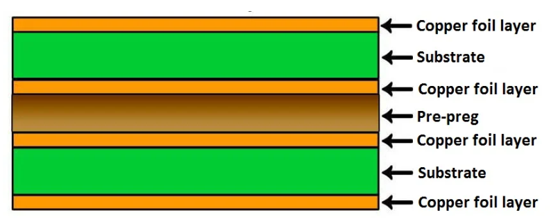
Copper Layer in PCB
Overview of the Copper Layer in PCBs
The copper layer in a printed circuit board (PCB) serves as the conductive backbone of the circuit, facilitating the flow of electrical signals between components and circuit elements. Copper is widely preferred for its excellent electrical conductivity, corrosion resistance, and ease of fabrication. The copper layer is typically deposited or laminated onto the substrate material to form conductive traces, pads, and planes, which interconnect the various components and elements of the circuit.
Role of Copper in Providing Conductivity for Circuit Traces
Copper plays a crucial role in providing electrical conductivity for circuit traces, which are the pathways that carry electrical signals between components on the PCB. The copper layer is etched or patterned to create intricate patterns of conductive traces that define the circuit’s functionality and connectivity. These traces carry signals, power, and ground connections, enabling the proper operation of electronic devices.
Copper’s high electrical conductivity allows signals to propagate efficiently with minimal loss, ensuring reliable signal transmission throughout the circuit. The thickness and width of copper traces are carefully designed to meet the electrical requirements of the circuit, such as signal integrity, current carrying capacity, and impedance control.
Interaction Between Substrate and Copper Layer
The interaction between the substrate material and the copper layer is essential for the overall performance and reliability of the PCB. The substrate provides mechanical support and electrical insulation for the copper layer, while the copper layer delivers conductivity and interconnection between circuit elements.
During PCB fabrication, the copper layer is bonded or deposited onto the substrate surface through processes such as electroplating, lamination, or deposition. The substrate material must have sufficient surface roughness and adhesion properties to ensure strong adhesion between the copper layer and the substrate.
Additionally, the thermal expansion coefficients (CTE) of the substrate material and the copper layer should be compatible to minimize the risk of delamination or mechanical stress-induced failures during temperature variations. Mismatched CTEs can lead to mechanical stress and warping, compromising the structural integrity and reliability of the PCB.
The substrate also influences the electrical properties of the copper traces, such as impedance and signal integrity. Variations in the dielectric constant (Dk) and thickness of the substrate material can affect the characteristic impedance of the traces and signal propagation speeds, leading to signal distortion or reflections.
Overall, the interaction between the substrate and the copper layer is critical for achieving optimal electrical performance, mechanical stability, and reliability in PCB designs. Careful consideration of material properties, fabrication processes, and design factors is necessary to ensure the successful integration of the copper layer within the PCB substrate.
PCB Material Selection
Factors to Consider When Selecting a PCB Substrate
Selecting the right substrate material is crucial for the performance, reliability, and manufacturability of a printed circuit board (PCB). Several factors should be considered during the material selection process:
- Application Requirements: Understanding the specific requirements of the application is paramount. Factors such as the temperature range in which the PCB will operate, the environmental conditions it will be exposed to (e.g., humidity, chemical exposure, vibration), and the frequency of signals transmitted through the PCB all play a significant role in determining the most suitable substrate material.
- Electrical Properties: The electrical properties of the substrate, including dielectric constant (Dk), dissipation factor (Df), and insulation resistance, are critical for signal integrity and electrical performance. High-frequency applications may require substrates with low Dk and Df values to minimize signal loss and distortion, while high insulation resistance is essential for preventing electrical leakage and ensuring reliability.
- Mechanical Properties: The mechanical properties of the substrate, such as tensile strength, thermal expansion coefficient (CTE), and moisture absorption, are vital for ensuring the structural integrity and reliability of the PCB. The substrate material should have adequate strength to withstand mechanical stresses during fabrication, assembly, and operation, as well as compatible thermal expansion properties to minimize the risk of warping or delamination.
- Thermal Management: Efficient heat dissipation is essential, especially in high-power applications or environments with elevated temperatures. Substrate materials with high thermal conductivity or good thermal stability help dissipate heat generated by electronic components, preventing overheating and ensuring reliable operation.
- Chemical Compatibility: Consideration should be given to the substrate material’s resistance to chemicals, solvents, and environmental contaminants that may come into contact with the PCB during its lifecycle. Chemical-resistant substrates help maintain the integrity and performance of the PCB in harsh operating environments.
- Fabrication Compatibility: The substrate material should be compatible with the PCB fabrication processes, including drilling, etching, soldering, and surface finishing. Some materials may require specialized processing techniques or equipment, which can impact manufacturing costs and lead times.
Application Requirements: Temperature Range, Operating Environment, Signal Frequency
The temperature range in which the PCB will operate influences the choice of substrate material, as different materials exhibit varying thermal stability and resistance to temperature extremes. For example, applications operating in high-temperature environments may require substrates with excellent thermal stability, such as polyimide or ceramic, to withstand elevated temperatures without degradation.
Similarly, the operating environment, including factors such as humidity, moisture, chemical exposure, and vibration, informs the selection of substrate material with appropriate environmental resistance properties. For harsh environments, substrates with high moisture resistance, chemical resistance, and mechanical durability are preferred to ensure long-term reliability.
The signal frequency transmitted through the PCB impacts signal integrity and requires substrates with low dielectric loss and consistent electrical properties, particularly at high frequencies. Materials with low dielectric constant (Dk) and low dissipation factor (Df) are preferred for high-frequency applications to minimize signal distortion and loss.
Cost Considerations and Availability
Cost considerations and material availability play a significant role in the selection process, especially for mass-produced or cost-sensitive applications. While certain substrate materials may offer superior performance or properties, they may also come at a higher cost or limited availability. Evaluating the trade-offs between performance, cost, and availability is essential to ensure the chosen substrate material aligns with budgetary constraints and production requirements.
Furthermore, considering the overall lifecycle cost of the PCB, including factors such as maintenance, reliability, and potential failure risks, is crucial for making informed decisions regarding material selection. Balancing performance requirements with cost-effectiveness helps optimize the overall value proposition of the PCB design.
Selecting the right substrate material for a PCB involves a comprehensive evaluation of application requirements, electrical and mechanical properties, thermal management capabilities, environmental considerations, fabrication compatibility, cost considerations, and material availability. By carefully assessing these factors and prioritizing the most critical requirements, designers can choose the optimal substrate material to ensure the successful design, performance, and reliability of the PCB for its intended application.
What is the Best Substrate for PCB?
Evaluation of Factors Influencing the Choice of Substrate
Selecting the best substrate for a printed circuit board (PCB) involves a comprehensive evaluation of various factors that influence the performance, reliability, and manufacturability of the PCB. Key factors to consider include:
- Application Requirements: Understanding the specific needs and operational parameters of the application is crucial. Factors such as temperature range, operating environment, signal frequency, power requirements, and reliability expectations play a significant role in determining the most suitable substrate material.
- Electrical Properties: The electrical properties of the substrate, including dielectric constant (Dk), dissipation factor (Df), and insulation resistance, directly impact signal integrity, power distribution, and electrical performance. Substrates with consistent electrical properties, low loss tangent, and high insulation resistance are preferred for high-speed digital, RF/microwave, and high-frequency applications.
- Mechanical Properties: Mechanical properties such as tensile strength, thermal expansion coefficient (CTE), and moisture absorption influence the structural integrity, dimensional stability, and reliability of the PCB. Substrates with high mechanical strength, low CTE, and minimal moisture absorption are essential for ensuring robustness and durability in demanding operating conditions.
- Thermal Management: Efficient heat dissipation is critical, particularly in high-power applications or environments with elevated temperatures. Substrates with high thermal conductivity, good thermal stability, and effective heat dissipation capabilities help mitigate thermal issues, prevent overheating, and ensure long-term reliability of the PCB.
- Chemical Compatibility: Consideration should be given to the substrate material’s resistance to chemicals, solvents, and environmental contaminants that may be encountered during the PCB’s lifecycle. Chemical-resistant substrates help maintain the integrity and performance of the PCB in harsh operating environments and facilitate ease of cleaning and maintenance.
- Fabrication Compatibility: The substrate material should be compatible with the PCB fabrication processes, including drilling, etching, soldering, and surface finishing. Materials that are easy to work with, exhibit good adhesion properties, and support standard fabrication techniques help streamline manufacturing workflows and minimize production costs.
Consideration of Specific Application Needs
Different applications have unique requirements and performance criteria, necessitating the selection of substrate materials tailored to specific application needs:
- Consumer Electronics: For consumer electronics applications, where cost-effectiveness, high-volume production, and compact form factors are priorities, substrates such as FR4 or CEM are commonly used due to their affordability, versatility, and compatibility with standard fabrication processes.
- Telecommunications: In telecommunications applications, which often involve high-frequency RF/microwave signals and stringent signal integrity requirements, substrates with low Dk and Df values, such as PTFE-based materials or high-frequency laminates, are preferred to minimize signal loss and distortion.
- Aerospace and Defense: Aerospace and defense applications demand substrates with exceptional reliability, mechanical robustness, thermal stability, and resistance to harsh environmental conditions, such as polyimide or ceramic substrates, which offer superior performance in extreme temperature, vibration, and humidity environments.
- Automotive Electronics: Automotive electronics require substrates with high thermal stability, mechanical durability, and resistance to temperature fluctuations and vibrations. Substrates such as FR4 or ceramic materials are commonly used in automotive PCBs to ensure reliability and longevity under challenging operating conditions.
Discussion on the Best Substrate Options for Different Scenarios
The best substrate option for a specific scenario depends on a combination of factors, including application requirements, performance criteria, environmental conditions, and cost considerations:
- High-Frequency Applications: For high-frequency applications requiring minimal signal loss and distortion, substrates with low Dk and Df values, such as PTFE-based materials (e.g., Rogers, Taconic) or specialized high-frequency laminates, are the best choice to ensure optimal signal integrity and performance.
- High-Power Applications: In high-power applications where efficient heat dissipation is critical, substrates with high thermal conductivity, such as metal-core PCBs (e.g., aluminum or copper clad laminates), ceramic substrates, or specialized thermal management materials, offer the best solution to effectively dissipate heat and prevent thermal issues.
- Flexibility and Miniaturization: For applications requiring flexibility, miniaturization, and lightweight construction, flexible substrates such as polyimide (e.g., Kapton) or rigid-flex PCBs offer the best solution to accommodate bending or folding, reduce space constraints, and enable integration into compact designs.
- Cost-Conscious Applications: In cost-conscious applications where affordability is a priority, substrates such as FR4 or CEM are the best choice due to their cost-effectiveness, widespread availability, and compatibility with standard fabrication processes, offering a balance of performance and cost.
The best substrate for a PCB depends on the specific requirements, performance criteria, and environmental conditions of the application. By carefully evaluating these factors and selecting the most suitable substrate material, designers can ensure the successful design, performance, and reliability of the PCB for its intended use case.
Function of Substrate in Electronics
Detailed Exploration of the Function of Substrate in Electronic Circuits
The substrate in electronic circuits serves as the foundation upon which various components and interconnections are built. It plays a crucial role in providing structural support, electrical insulation, and facilitating the interconnection of electronic components to form functional circuits. Let’s delve into its functions in more detail:
- Structural Support: The substrate provides mechanical support for mounting and securing electronic components, such as integrated circuits (ICs), resistors, capacitors, and connectors. It forms the physical framework that holds the components in place, ensuring proper alignment and spacing for reliable operation. Additionally, the substrate helps distribute mechanical stresses and vibrations encountered during handling, assembly, and operation, safeguarding the integrity of the electronic assembly.
- Electrical Insulation: The substrate material serves as an electrical insulator, preventing unintended electrical contact between conductive elements, such as copper traces or layers, within the circuit. By isolating conductive elements from each other, the substrate minimizes the risk of short circuits, signal interference, and electrical leakage, ensuring the integrity and functionality of the circuit. Effective electrical insulation is essential for maintaining reliable performance and preventing electrical hazards in electronic devices.
- Interconnection of Components: The substrate facilitates the interconnection of electronic components through conductive traces, vias, and pads embedded within or deposited onto its surface. These conductive pathways establish electrical connections between components, enabling the transmission of signals, power, and ground references throughout the circuit. The substrate material should possess good adhesion properties and compatibility with fabrication processes to ensure reliable and durable interconnections.
Importance in Providing Structural Support and Electrical Insulation
The substrate’s role in providing structural support and electrical insulation is paramount for the overall performance, reliability, and safety of electronic circuits:
- Structural Support: The substrate’s mechanical strength and rigidity are essential for withstanding mechanical stresses and maintaining the integrity of the electronic assembly. It prevents components from shifting or becoming dislodged during handling, shipping, and operation, reducing the risk of damage or malfunction. Proper structural support ensures the long-term durability and robustness of electronic devices, particularly in rugged or harsh environments.
- Electrical Insulation: Effective electrical insulation provided by the substrate prevents electrical shorts, leakage, and signal interference, safeguarding the functionality and reliability of the circuit. Insulating properties are crucial for preventing accidental contact between conductive elements, minimizing the risk of electrical hazards, malfunctions, and damage to sensitive components. Reliable electrical insulation enhances the safety and performance of electronic devices, especially in high-voltage or high-current applications.
Impact on Signal Integrity and Reliability
The substrate material significantly influences signal integrity and reliability in electronic circuits:
- Signal Integrity: The substrate’s electrical properties, such as dielectric constant (Dk), dissipation factor (Df), and impedance characteristics, affect signal propagation, attenuation, and distortion. Variations in substrate properties can lead to signal reflections, impedance mismatches, and loss of signal integrity, impacting the accuracy and reliability of transmitted signals. Maintaining consistent electrical properties across the substrate is essential for preserving signal integrity and ensuring accurate data transmission in electronic circuits.
- Reliability: The substrate’s mechanical and electrical properties directly impact the reliability and longevity of electronic devices. Mechanical stability, thermal management capabilities, and resistance to environmental factors influence the PCB’s resistance to mechanical stress, thermal cycling, moisture absorption, and chemical exposure, which can lead to degradation or failure over time. A robust substrate design enhances the reliability and operational lifespan of electronic devices, minimizing downtime, maintenance costs, and warranty claims.
The substrate in electronic circuits plays a multifaceted role in providing structural support, electrical insulation, and facilitating reliable interconnections between components. Its functions are critical for ensuring the structural integrity, electrical performance, signal integrity, and reliability of electronic devices across various applications and operating conditions. By selecting appropriate substrate materials and designs, designers can optimize the performance, longevity, and safety of electronic circuits for their intended applications.
Difference Between IC Substrate and PCB
Differentiation between IC Substrate and Traditional PCB Substrate
While both IC (Integrated Circuit) substrates and traditional PCB (Printed Circuit Board) substrates serve as platforms for electronic components, they have distinct roles, designs, and applications:
- IC Substrate: IC substrates, also known as chip carriers or semiconductor substrates, are specialized substrates designed to mount, interconnect, and provide electrical connectivity to integrated circuits (ICs) or semiconductor devices. They are typically smaller in size and thinner compared to traditional PCB substrates and are optimized for high-density integration of semiconductor components.
- Traditional PCB Substrate: Traditional PCB substrates serve as the foundation for assembling electronic components, including ICs, resistors, capacitors, and connectors, to form functional circuits. They are available in various sizes, shapes, and configurations and are designed to accommodate a wide range of electronic devices and applications.
Role and Design Considerations for IC Substrates
IC substrates play a crucial role in enabling the integration, electrical connectivity, and thermal management of semiconductor devices. Key design considerations for IC substrates include:
- Interconnection Density: IC substrates are designed to accommodate high-density interconnections, fine pitch bonding, and complex routing configurations to accommodate the increasing integration and miniaturization of semiconductor components.
- Signal Integrity: Ensuring reliable signal transmission and minimizing signal loss, noise, and crosstalk are paramount in IC substrate design. Signal integrity considerations include impedance control, routing optimization, and minimizing parasitic effects to preserve signal quality and performance.
- Thermal Management: Effective heat dissipation is critical for maintaining the temperature of semiconductor devices within safe operating limits. IC substrates incorporate thermal vias, thermal pads, and heat sinks to dissipate heat generated by ICs, preventing thermal issues and ensuring device reliability.
- Material Selection: IC substrates utilize materials with specific electrical, mechanical, and thermal properties tailored to semiconductor applications. Substrate materials may include ceramics, organic substrates (e.g., FR4, BT resin), or specialized high-performance materials (e.g., silicon, glass, metal-core laminates) depending on the application requirements.
Comparison of Materials and Manufacturing Processes
Materials and manufacturing processes for IC substrates and traditional PCB substrates differ based on their respective design requirements and performance objectives:
- Materials: IC substrates often utilize advanced materials such as ceramics (e.g., alumina, aluminum nitride), organic substrates (e.g., BT resin, FR4), or specialized laminates (e.g., silicon, glass, metal-core laminates) tailored to semiconductor applications. Traditional PCB substrates typically use standard materials such as FR4, CEM, polyimide, or metal-core laminates optimized for general-purpose electronic assemblies.
- Manufacturing Processes: IC substrates require specialized manufacturing processes, including photolithography, thin-film deposition, laser drilling, and metallization techniques, to achieve high-precision features, fine pitch bonding, and complex routing configurations. Traditional PCB substrates utilize standard fabrication processes such as etching, drilling, plating, solder mask application, and surface finishing techniques compatible with mass production and assembly.
While IC substrates and traditional PCB substrates share common functions as platforms for electronic components, they have distinct roles, designs, materials, and manufacturing processes tailored to their respective applications in semiconductor packaging and general-purpose electronic assemblies. Understanding the differences between IC substrates and traditional PCB substrates is essential for selecting the most suitable substrate platform for specific electronic device designs and applications.
How to Select a PCB Substrate?
Selecting the right PCB substrate is a critical decision that impacts the performance, reliability, and manufacturability of electronic devices. Here’s a step-by-step guide to help you navigate the process effectively:
1. Define Application Requirements:
- Identify the specific needs and operational parameters of the application, including temperature range, operating environment, signal frequency, power requirements, and reliability expectations.
- Consider factors such as electrical performance, mechanical robustness, thermal management, chemical resistance, and environmental durability.
2. Evaluate Material Properties:
- Understand the key material properties of PCB substrates, including electrical properties (dielectric constant, dissipation factor, insulation resistance), mechanical properties (tensile strength, thermal expansion coefficient, moisture absorption), thermal conductivity, chemical resistance, and dimensional stability.
- Assess how these material properties align with the application requirements and performance criteria.
3. Consider Signal Integrity and Reliability:
- Evaluate the impact of substrate material properties on signal integrity, including signal propagation, attenuation, distortion, impedance control, and electromagnetic interference (EMI).
- Ensure that the selected substrate material maintains reliable electrical performance and signal integrity throughout the intended operating conditions.
4. Assess Thermal Management Needs:
- Determine the thermal management requirements of the application, including heat dissipation, thermal conductivity, and temperature stability.
- Select a substrate material with appropriate thermal properties to dissipate heat effectively and prevent thermal issues, ensuring reliable operation under varying temperature conditions.
5. Analyze Cost and Availability:
- Consider the cost-effectiveness and availability of different substrate materials, taking into account material costs, fabrication costs, lead times, and supplier availability.
- Evaluate the overall lifecycle cost of the PCB, including maintenance, reliability, and potential failure risks, to make informed decisions regarding material selection.
6. Collaborate with Designers and Material Suppliers:
- Foster collaboration between PCB designers and material suppliers to optimize substrate selection based on application requirements and material capabilities.
- Seek input from material suppliers regarding substrate options, performance characteristics, fabrication processes, and material availability.
- Leverage the expertise of material suppliers to identify suitable substrate materials, address technical challenges, and optimize the design for performance, reliability, and manufacturability.
7. Prototype and Test:
- Develop prototypes using selected substrate materials to validate performance, functionality, and reliability under real-world conditions.
- Conduct thorough testing and evaluation of prototype PCBs to assess electrical performance, signal integrity, thermal management, mechanical robustness, and environmental durability.
- Iterate the design and material selection process based on testing results and feedback to refine the PCB design and optimize performance.
By following this step-by-step guide, designers can effectively select the right PCB substrate that meets the specific requirements of their application, ensures reliable performance, and enhances the overall quality and reliability of electronic devices. Collaboration between designers and material suppliers is essential for leveraging expertise, optimizing substrate selection, and achieving successful outcomes in PCB design and manufacturing.
FAQs About what is substrate in pcb
The best substrate for a PCB depends on the specific requirements of the application. Common substrate materials include FR4, polyimide, and ceramics. FR4 is widely used due to its affordability, versatility, and compatibility with standard fabrication processes. Polyimide substrates offer flexibility and high-temperature resistance, making them suitable for flexible PCBs and applications requiring thermal stability. Ceramics provide excellent thermal conductivity and mechanical strength, making them ideal for high-power and high-frequency applications.
The substrate in electronics serves several essential functions:
Structural Support: It provides a physical framework for mounting and securing electronic components, ensuring proper alignment and spacing.
Electrical Insulation: The substrate material prevents unintended electrical contact between conductive elements, minimizing the risk of short circuits and ensuring electrical safety.
Interconnection: The substrate facilitates the interconnection of electronic components through conductive traces, vias, and pads, enabling the transmission of signals, power, and ground references throughout the circuit.
IC Substrate: IC substrates, also known as chip carriers, are specialized substrates designed to mount, interconnect, and provide electrical connectivity to integrated circuits (ICs) or semiconductor devices. They are optimized for high-density integration of semiconductor components and feature fine pitch bonding, complex routing configurations, and thermal management features.
PCB (Printed Circuit Board): PCB substrates serve as the foundation for assembling electronic components to form functional circuits. They are available in various sizes, shapes, and configurations and accommodate a wide range of electronic devices and applications. PCB substrates utilize standard fabrication processes and materials tailored to general-purpose electronic assemblies.
To select a PCB substrate:
Define application requirements, including temperature range, operating environment, signal frequency, and reliability expectations.
Evaluate material properties such as electrical, mechanical, and thermal characteristics to ensure alignment with application needs.
Consider signal integrity, thermal management, cost, and availability when comparing substrate options.
Collaborate with PCB designers and material suppliers to optimize substrate selection based on application requirements and material capabilities.
Develop prototypes and conduct testing to validate performance, functionality, and reliability under real-world conditions, iterating the design and material selection process as needed.

