
What is a Glass Substrate: Understanding Its Role and Importance
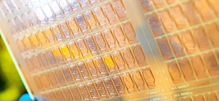
What is a Glass Substrate? A glass substrate is a thin, flat sheet of glass used as a foundational material in various technological applications. It offers exceptional dimensional stability, optical clarity, and smoothness, making it an ideal choice for high-precision processes. Glass substrates are widely used in fields like semiconductor manufacturing, display technologies (e.g., LCD and OLED screens), and photovoltaic cells. Their excellent thermal and chemical resistance ensures reliability in demanding environments. Additionally, glass substrates can support advanced coatings or patterns for specific functionalities, such as conducting layers or optical filters. With the rise of microelectronics and nanotechnology, glass substrates are becoming increasingly essential in enabling compact, high-performance devices. Their versatility drives innovation across industries.
Understanding Glass Substrates: What Is a Glass Substrate?
To grasp the significance of advanced technology in modern industries, it is crucial to ask: what is a glass substrate? At its core, a glass substrate is a meticulously engineered, thin, and flat piece of glass that serves as the foundational platform for many high-tech applications. This section dives deep into its definition, composition, and versatile applications across various industries.
Definition and Composition
When we discuss what is a glass substrate, it is important to consider both its physical and chemical properties. A glass substrate is a base layer upon which other materials, such as metals, semiconductors, or optical coatings, are deposited or fabricated. Its primary role is to provide structural support while ensuring the precise conditions needed for complex manufacturing processes.
-
Composition:
- Base Material: Glass substrates are typically made from high-purity materials, including borosilicate glass, aluminosilicate glass, or quartz. These materials are chosen for their exceptional thermal and mechanical stability.
- Coatings: Depending on the application, glass substrates may have additional coatings that enhance properties like electrical conductivity, anti-reflective performance, or scratch resistance.
-
Physical Properties:
- Flatness and Smoothness: Critical for applications where surface uniformity ensures optimal performance, such as semiconductor manufacturing.
- Optical Clarity: Transparent or translucent, depending on the intended use, making it ideal for display technologies and optics.
- Durability: Resistant to thermal shock, mechanical stress, and chemical corrosion, ensuring longevity even in demanding environments.
Applications in Different Industries
Now that we understand what is a glass substrate, its vast array of applications becomes evident. Glass substrates play a pivotal role in advancing technology across multiple sectors:
-
Electronics:
Glass substrates are indispensable in the production of displays for devices like smartphones, televisions, and tablets. Thin-film transistors (TFTs) used in LCD and OLED displays are built on these substrates, ensuring high resolution and energy efficiency. -
Semiconductor Industry:
In microelectronics, glass substrates provide the stable base required for creating precise and compact circuits. They are used in photomask substrates for lithography and as insulating layers in chips. -
Photovoltaics:
Glass substrates are vital in solar panel manufacturing, where they serve as the base for thin-film solar cells. Their durability and optical properties contribute to the efficiency and lifespan of solar modules. -
Optical Devices:
The optical clarity and smoothness of glass substrates make them essential for camera sensors, lenses, and other imaging technologies. Precision is crucial in these applications, and glass substrates deliver the required performance. -
Healthcare and Biotechnology:
In the medical field, glass substrates are used in diagnostic tools like lab-on-a-chip devices and microfluidic systems. Their biocompatibility and chemical resistance make them ideal for these cutting-edge applications.

Glass Substrate in Semiconductors
Importance in Semiconductor Manufacturing
Role in Chip Fabrication
Glass substrates play a critical role in semiconductor manufacturing, serving as the foundation upon which integrated circuits (ICs) and other microelectronic devices are built. During chip fabrication, various semiconductor materials and layers are deposited onto the surface of the glass substrate using techniques such as chemical vapor deposition (CVD) and physical vapor deposition (PVD). These processes enable the creation of intricate patterns and structures necessary for the functioning of electronic circuits.
Benefits for Semiconductor Performance
Glass substrates offer several key benefits that contribute to the performance and reliability of semiconductor devices:
- Electrical Insulation: Glass substrates provide excellent electrical insulation, reducing the risk of signal interference and leakage currents within semiconductor devices.
- Thermal Stability: The thermal stability of glass substrates ensures that semiconductor devices can operate reliably over a wide range of temperatures, without the risk of warping or degradation.
- Surface Smoothness: The flat and smooth surface of glass substrates allows for precise deposition of semiconductor materials and layers, enabling the creation of high-quality integrated circuits with minimal defects.
Examples and Case Studies
Intel’s Use of Glass Substrates
Intel, a leading semiconductor manufacturer, has been actively exploring the use of glass substrates in its chip fabrication processes. The company has recognized the potential benefits of glass substrates, such as improved thermal management and enhanced performance, particularly in high-performance computing applications. By leveraging glass substrates, Intel aims to optimize the design and manufacturing of its next-generation processors, ensuring greater efficiency and reliability.
TSMC’s Advancements with Glass Substrates
Taiwan Semiconductor Manufacturing Company (TSMC), the world’s largest semiconductor foundry, has also made significant advancements in the use of glass substrates. TSMC has developed innovative techniques for integrating glass substrates into its chip packaging processes, enabling the creation of more compact and energy-efficient semiconductor devices. By incorporating glass substrates into its manufacturing processes, TSMC aims to address the growing demand for high-performance chips in applications such as artificial intelligence, 5G communications, and automotive electronics.
Glass substrates play a crucial role in semiconductor manufacturing, offering benefits such as electrical insulation, thermal stability, and surface smoothness. Companies like Intel and TSMC are actively exploring the use of glass substrates to enhance the performance and reliability of their semiconductor devices, paving the way for continued advancements in the industry.
Benefits of Glass Substrates
Enhanced Performance
Improved Electrical Properties
Glass substrates offer superior electrical insulation compared to other substrate materials like silicon or ceramics. This insulation reduces electrical noise and leakage currents within semiconductor devices, leading to improved signal integrity and overall performance.
Better Thermal Management
The thermal stability of glass substrates allows semiconductor devices to dissipate heat more efficiently, preventing overheating and thermal degradation. This ensures consistent performance and reliability, especially in high-power applications where thermal management is critical.
Mechanical Properties
Durability and Stability
Glass substrates are highly durable and stable, capable of withstanding mechanical stress and environmental factors such as temperature fluctuations and humidity. This durability ensures the long-term reliability of semiconductor devices, even in harsh operating conditions.
Lightweight Nature
Despite their durability, glass substrates are lightweight compared to alternative materials like silicon or metal. This lightweight nature reduces the overall weight of semiconductor devices, making them more portable and suitable for applications where weight is a concern, such as mobile devices and automotive electronics.
Precision and Scalability
High-Precision Manufacturing Capabilities
Glass substrates can be manufactured with extremely high precision, allowing for the creation of intricate patterns and structures with micron-level accuracy. This precision is essential for the fabrication of advanced semiconductor devices, where even minor deviations can impact performance.
Scalability for Mass Production
Glass substrates offer scalability for mass production, allowing semiconductor manufacturers to produce large quantities of devices with consistent quality and performance. This scalability is crucial for meeting the growing demand for semiconductor devices in various industries, from consumer electronics to automotive and industrial applications.
Glass substrates offer a range of benefits that contribute to the enhanced performance, durability, and scalability of semiconductor devices. From improved electrical properties and thermal management to precision manufacturing capabilities, glass substrates play a vital role in advancing technology and driving innovation in the semiconductor industry.

Glass Substrate Manufacturers
Leading Manufacturers
Overview of Major Players in the Market
Several companies specialize in the manufacturing of glass substrates for various industries, including semiconductor manufacturing, optics, and advanced packaging. Some of the leading manufacturers in the market include:
- Corning Incorporated: Corning is a renowned manufacturer of specialty glass and ceramics, offering a wide range of glass substrates for applications such as displays, optical devices, and semiconductor packaging.
- Asahi Glass Co., Ltd. (AGC): AGC is a global glass manufacturing company that produces glass substrates for semiconductors, displays, and electronic components. The company’s advanced glass technologies cater to the needs of high-tech industries worldwide.
- Nippon Electric Glass Co., Ltd. (NEG): NEG specializes in the production of glass substrates for electronic devices, including semiconductors, photovoltaic cells, and sensors. The company’s innovative glass solutions contribute to the development of cutting-edge technologies.
- Schott AG: Schott is a leading manufacturer of specialty glass and glass-ceramics, providing glass substrates for applications such as optics, photonics, and semiconductor packaging. The company’s high-quality glass products meet the stringent requirements of various industries.
Intel, TSMC, and Samsung’s Roles
Intel’s Use of Glass Substrates
Intel has been actively exploring the use of glass substrates in semiconductor manufacturing to enhance the performance and reliability of its chips. The company’s research and development efforts focus on optimizing the design and manufacturing processes to leverage the benefits of glass substrates, such as improved thermal management and electrical insulation.
TSMC’s Advancements with Glass Substrates
TSMC, as a leading semiconductor foundry, has made significant advancements in integrating glass substrates into its chip packaging processes. The company’s innovative packaging technologies, such as System on Integrated Chips (SoIC) and InFO (Integrated Fan-Out), utilize glass substrates to achieve higher levels of miniaturization and integration in semiconductor devices.
Samsung’s Utilization of Glass Substrates
Samsung, a major player in the semiconductor industry, also recognizes the potential of glass substrates for enhancing the performance and reliability of its chips. The company’s research and development efforts focus on integrating glass substrates into its advanced packaging solutions, enabling the development of more compact and energy-efficient semiconductor devices.
Manufacturing Processes
Key Steps in Glass Substrate Production
The manufacturing process of glass substrates involves several key steps, including:
- Glass Melting: Raw materials such as silica sand, soda ash, and limestone are melted together in a furnace to form molten glass.
- Glass Forming: The molten glass is formed into flat sheets using processes such as float glass or fusion draw.
- Surface Treatment: The glass sheets undergo surface treatments to enhance properties such as smoothness, transparency, and chemical resistance.
- Cutting and Shaping: The glass sheets are cut and shaped into precise dimensions using diamond saws or laser cutting techniques.
- Cleaning and Inspection: The glass substrates are thoroughly cleaned and inspected for defects before being packaged for shipment.
Innovations in Manufacturing Techniques
Recent advancements in glass substrate manufacturing include the development of ultra-thin glass substrates, advanced surface treatments for improved performance, and novel shaping techniques for complex geometries. Additionally, the integration of automation and robotics in manufacturing processes has led to increased efficiency and precision in producing glass substrates for high-tech applications.
In conclusion, leading manufacturers such as Corning, AGC, NEG, and Schott play a crucial role in supplying high-quality glass substrates for various industries. Companies like Intel, TSMC, and Samsung are actively exploring the use of glass substrates to enhance the performance and reliability of their semiconductor devices, driving innovation and advancement in the industry.

Glass Substrates in Advanced Packaging
Technological Integration
How Glass Substrates are Used in Advanced Packaging
In advanced packaging, glass substrates play a crucial role in enabling innovative packaging solutions that enhance miniaturization, integration, and performance of semiconductor devices. Glass substrates are utilized as a foundational layer in various packaging technologies, including System in Package (SiP), System on Chip (SoC), and 3D packaging architectures.
Benefits for Miniaturization and Integration
Glass substrates offer several benefits that contribute to the miniaturization and integration of semiconductor devices:
- Thinness: Glass substrates can be manufactured with ultra-thin profiles, allowing for the creation of compact and lightweight packages.
- High Density: Glass substrates enable the integration of multiple chips and components in a single package, increasing device functionality and performance.
- High Precision: The flatness and uniformity of glass substrates facilitate the precise alignment and bonding of chips and interconnects, ensuring reliable electrical connections and signal integrity.
Examples of Advanced Packaging Solutions
Specific Products and Technologies Utilizing Glass Substrates
- Fan-Out Wafer-Level Packaging (FOWLP): FOWLP is an advanced packaging technique that uses glass substrates as carrier wafers for redistributing and interconnecting individual dies. Glass substrates offer excellent thermal and mechanical properties, enabling the creation of thin and robust packages suitable for high-performance applications.
- Embedded Wafer-Level Ball Grid Array (eWLB): eWLB is a packaging technology that integrates chips directly into a glass substrate, eliminating the need for traditional package substrates. Glass substrates provide superior electrical and thermal performance, enabling higher levels of integration and improved reliability in semiconductor devices.
- Wafer-Level Chip Scale Package (WLCSP): WLCSP is a packaging technique that mounts bare semiconductor dies directly onto a glass substrate, eliminating the need for wire bonding or flip-chip assembly. Glass substrates offer excellent electrical insulation and thermal conductivity, enabling compact and efficient packaging solutions for mobile and IoT devices.
- Chip-on-Glass (COG): COG is a packaging method where semiconductor chips are directly bonded to a glass substrate, typically for display applications. Glass substrates provide a stable and flat surface for mounting display driver chips, enabling high-resolution and high-definition displays in smartphones, tablets, and other electronic devices.
Glass substrates play a vital role in advanced packaging solutions, enabling miniaturization, integration, and improved performance of semiconductor devices. Technologies such as FOWLP, eWLB, WLCSP, and COG leverage the unique properties of glass substrates to create innovative packaging solutions that meet the evolving demands of the semiconductor industry.
Packaging of Glass Substrates
Packaging Techniques
Methods Used for Packaging Glass Substrates
Packaging of glass substrates involves several techniques to ensure their protection and integrity during transportation and handling. Some common packaging methods include:
- Individual Packaging: Each glass substrate is individually packaged in protective materials such as foam or plastic trays to prevent physical damage and contamination.
- Bulk Packaging: Multiple glass substrates are stacked and packaged together in trays or containers, separated by protective materials to prevent scratching and breakage.
- Vacuum Packaging: Glass substrates are sealed in vacuum-sealed bags or containers to protect them from moisture, dust, and other environmental contaminants.
Protection and Handling During Transportation
Glass substrates are highly sensitive to mechanical stress and environmental factors, making proper handling and transportation essential to prevent damage and ensure their integrity. During transportation, glass substrates should be:
- Handled with Care: Glass substrates should be handled gently to avoid impacts, drops, and vibrations that could cause breakage or surface damage.
- Protected from Moisture and Humidity: Glass substrates should be stored and transported in dry, climate-controlled environments to prevent moisture absorption and potential damage to the substrate surface.
- Secured During Transit: Glass substrates should be securely packaged and properly labeled to prevent shifting or movement during transit, reducing the risk of breakage or loss.
Importance of Proper Packaging
Ensuring Integrity and Functionality
Proper packaging of glass substrates is essential to ensure their integrity and functionality throughout the manufacturing and assembly processes. Improper handling or packaging can lead to surface damage, contamination, or breakage, compromising the performance and reliability of semiconductor devices.
Reducing Damage and Contamination Risks
Effective packaging techniques help to minimize the risk of damage and contamination during transportation and handling. By providing adequate protection and insulation, proper packaging helps to safeguard glass substrates from scratches, abrasions, moisture, and other environmental hazards that could affect their performance and longevity.
In conclusion, proper packaging of glass substrates is essential to protect their integrity and functionality during transportation and handling. By employing appropriate packaging techniques, semiconductor manufacturers can minimize the risk of damage and contamination, ensuring the reliability and performance of glass substrates in advanced packaging applications.

Substrates in Optics and CPUs
Optical Applications
Role of Substrates in Optical Devices
Substrates play a critical role in the manufacturing of various optical devices, providing a stable platform for the deposition and fabrication of optical components. In optical devices such as lenses, displays, and sensors, substrates serve as the foundation upon which optical elements are deposited, bonded, or etched to create precise and functional devices.
Examples in Lenses, Displays, and Sensors
- Lenses: In optical lenses, substrates serve as the base material onto which lens elements are ground, polished, and coated to achieve desired optical properties such as refractive index, transmission, and dispersion.
- Displays: Substrates are used in display technologies such as liquid crystal displays (LCDs), organic light-emitting diode (OLED) displays, and microelectromechanical systems (MEMS) displays. Glass substrates, in particular, are commonly used as the substrate material due to their transparency, flatness, and mechanical stability.
- Sensors: In optical sensors such as image sensors and photodetectors, substrates provide a stable platform for the deposition of photosensitive materials or semiconductor devices. Glass substrates are often utilized in sensor fabrication for their optical clarity and compatibility with semiconductor processes.
Substrates in Chips and CPUs
Explanation of Substrate Role in Chip Manufacturing
In semiconductor manufacturing, substrates serve as the foundation upon which semiconductor devices are built. The substrate, typically made of silicon, provides mechanical support and electrical connections for the semiconductor components, such as transistors, diodes, and interconnects.
Specifics About CPU Substrates
In central processing units (CPUs), the substrate plays a crucial role in providing electrical connectivity between the CPU die and the motherboard. The CPU substrate, also known as the package substrate or package carrier, is typically made of a high-performance laminate material such as fiberglass-reinforced epoxy resin. It features a complex network of conductive traces and vias that route signals between the CPU die and the external pins or pads.
The CPU substrate also incorporates other essential components such as power delivery networks, decoupling capacitors, and thermal management solutions to ensure optimal performance and reliability of the CPU. Advanced packaging technologies, such as flip-chip packaging and ball grid array (BGA) packaging, are commonly employed in CPU substrates to achieve high levels of integration, performance, and thermal efficiency.
Substrates play integral roles in both optical devices and semiconductor devices such as CPUs. Whether in lenses, displays, sensors, or CPU packages, substrates provide the necessary foundation for the fabrication, integration, and functionality of these advanced technologies.
Get a Quote Now
FAQs About what is a glass substrate
Benefits of Glass Substrate: Glass substrates offer various benefits such as superior electrical insulation, excellent thermal management, durability, lightweight nature, precision manufacturing capabilities, and scalability for mass production. These properties make glass substrates ideal for applications in semiconductors, optics, and advanced packaging.
Substrate in Optics: In optics, a substrate refers to the underlying material upon which optical components or devices are fabricated or deposited. It provides a stable foundation for the construction of lenses, displays, sensors, and other optical systems.
the base material upon which semiconductor devices are built. It provides mechanical support and electrical connections for the semiconductor components, such as transistors and interconnects.
The substrate of a CPU, also known as the package substrate or package carrier, is a critical component that provides electrical connectivity between the CPU die and the motherboard. It is typically made of a high-performance laminate material and features a complex network of conductive traces and vias to route signals between the CPU die and the external pins or pads. The CPU substrate also incorporates other essential components such as power delivery networks, decoupling capacitors, and thermal management solutions to ensure optimal performance and reliability of the CPU.

